Side wall structure construction method

A technology of a sidewall structure and a manufacturing method, which is applied in the manufacture of semiconductor/solid-state devices, electrical components, semiconductor devices, etc., can solve the problems of silicon damage, large stress, and impact on device performance of semiconductor substrates.

Inactive Publication Date: 2012-10-03
SHANGHAI HUALI MICROELECTRONICS CORP
View PDF4 Cites 2 Cited by
  • Summary
  • Abstract
  • Description
  • Claims
  • Application Information

AI Technical Summary

Problems solved by technology

In order to make a side wall structure with a small thickness, the existing technology uses a single thin dielectric layer to make the side wall structure, such as using a single thin silicon oxide layer or a silicon nitride layer to make the side wall structure, but using a single thin silicon oxide layer Fabrication of the sidewall structure, in the pro

Method used


Image

  • Side wall structure construction method
  • Side wall structure construction method
  • Side wall structure construction method

Examples


Embodiment Construction

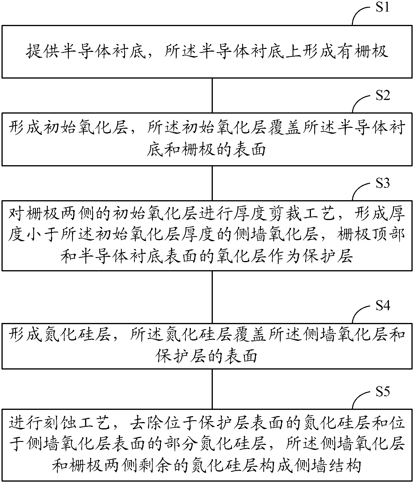
[0027] For processes with a feature size of 65 nanometers and above, the thickness of the sidewall structure is relatively large, usually greater than 100 angstroms, and the manufacturing process of the sidewall structure is relatively easy. However, as the feature size of the device is reduced, the inventor found that it is impossible to form a sidewall structure with a smaller thickness using the existing technology. If a single silicon oxide layer is used to make the sidewall structure, the process of etching the silicon oxide layer to form the sidewall structure will cause silicon damage to the semiconductor substrate (Siloss). If a single silicon nitride layer is used to make the sidewall structure, Then the silicon nitride layer causes greater stress on the device, thereby affecting the performance of the device. Therefore, the inventor considers using a silicon oxide layer and a silicon nitride layer to make the sidewall structure. In order to ensure that the thickness o...


PUM

PropertyMeasurementUnit
Thicknessaaaaaaaaaa
Thicknessaaaaaaaaaa
Thicknessaaaaaaaaaa

Abstract

The invention provides a side wall structure construction method which comprises the following steps: providing a semiconductor substrate, wherein a grid electrode is formed on the semiconductor substrate; forming an initial oxidation layer which covers the surfaces of the semiconductor substrate and the grid electrode; thinning the initial oxidation layer on two sides of the grid electrode so as to form a side wall oxidation layer of which the thickness is less than that of the initial oxidation layer, wherein the oxidation layers at the top of the grid electrode and the surface of the semiconductor substrate serve as protection layers; forming silicon nitride layers which cover the surfaces of the side wall oxidation layer and the protection layers; and carrying out an etching process so as to remove the silicon nitride layers positioned on the surfaces of the protection layers and the partial silicon nitride layer on the surface of the side wall oxidation layer, wherein the side wall oxidation layer and the residual silicon nitride layers on the two sides of the grid electrode together form a side wall structure. Due to the adoption of the wall side wall structure construction method provided by the invention, the side wall structure with smaller thickness (50-60 angstrom) can be constructed.

Description

Technical field [0001] The invention relates to a manufacturing method of a semiconductor device, in particular to a manufacturing method of a sidewall structure. Background technique [0002] In the process of transistor fabrication, it is usually necessary to fabricate sidewall structures on both sides of the gate using a deposition process and an etching process. For transistors with a device feature size above 55 nanometers, the width of the sidewall structure is usually greater than 100 angstroms. As the feature size of the device continues to decrease, the thickness of the sidewall structure needs to be reduced. In order to fabricate a sidewall structure with a small thickness, the prior art uses a single thin dielectric layer to fabricate the sidewall structure. For example, a single thin silicon oxide layer or a silicon nitride layer is used to fabricate the sidewall structure, but a single thin silicon oxide layer is used. The sidewall structure is made. In the process...

Claims


Application Information

Patent Timeline
IPC IPC(8): H01L21/28H01L21/336H01L21/311
Inventor 李全波张瑜
Owner SHANGHAI HUALI MICROELECTRONICS CORP
Why Eureka
Try Eureka