Memory architecture of 3d array with improved uniformity of bit line capacitances

A technology of memory and memory unit, which is applied in the direction of electric solid-state devices, circuits, electrical components, etc., and can solve problems such as numerical difficulties

Active Publication Date: 2012-10-03
MACRONIX INT CO LTD
View PDF4 Cites 17 Cited by
  • Summary
  • Abstract
  • Description
  • Claims
  • Application Information

AI Technical Summary

Problems solved by technology

The different bit line capacitances of these different bit lines make it difficult to sense the value stored in the memory cell

Method used


Image

  • Memory architecture of 3d array with improved uniformity of bit line capacitances
  • Memory architecture of 3d array with improved uniformity of bit line capacitances
  • Memory architecture of 3d array with improved uniformity of bit line capacitances

Examples


Embodiment Construction

[0135] A detailed description of the embodiments with reference to the accompanying drawings will be provided below.

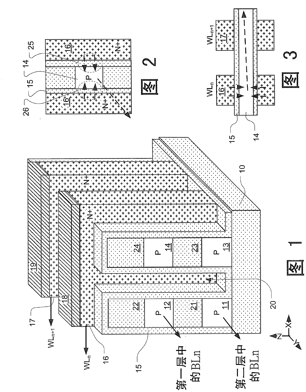
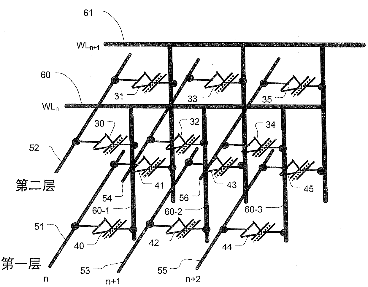
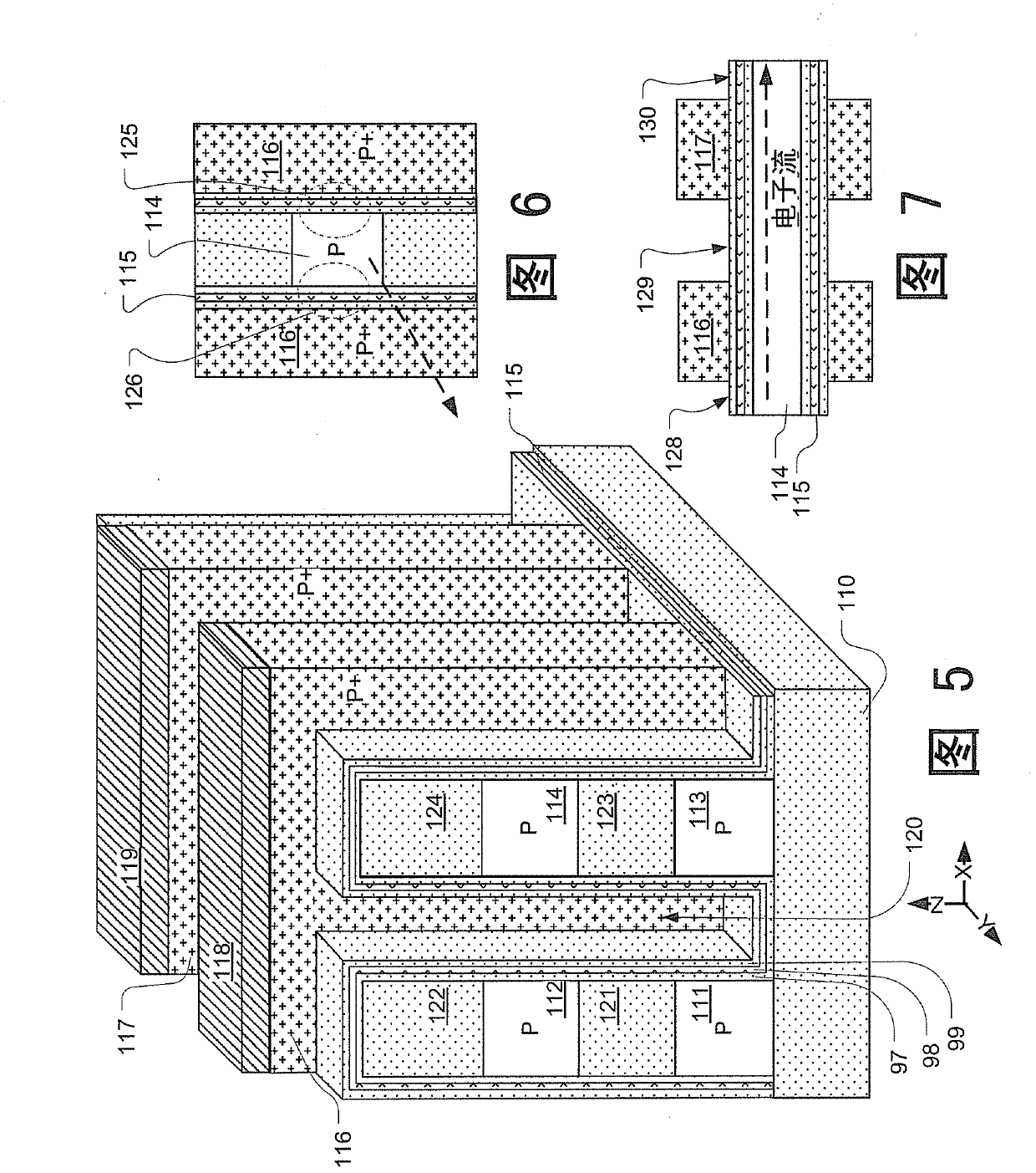
[0136] figure 1 A perspective view of a 2×2 portion of a 3D programmable resistive memory array with fill material removed from the drawing to reveal the semiconductor strip stacks and vertical word lines that make up the 3D array. In this drawing, only two planes are shown. However, the number of planes can be extended to be very large. Such as figure 1 As shown, the memory array is fabricated on an integrated circuit substrate having an insulating layer 10 based on a semiconductor or other structure (not shown). The memory array includes multiple stacks of semiconductor strips 11 , 12 , 13 and 14 separated by insulating material 21 , 22 , 23 and 24 . The plurality of stacks are in the shape of ridges extending along the Y axis, as shown, such that semiconductor strips 11-14 can be configured as strings of memory cells. Semiconductor strips 11 and 13 can...


PUM


Abstract

A 3D integrated circuit memory array has a plurality of plane positions. Multiple bit line structures have a multiple sequences of multiple plane positions. Each sequence characterizes an order in which a bit line structure couples the plane positions to bit lines. Each bit line is coupled to at least two different plane positions to access memory cells at two or more different plane positions.

Description

technical field [0001] The present invention is a high density memory device, and in particular a memory device in which multiple planes of memory cells are used to provide a 3D array. Background technique [0002] As the critical dimensions of devices in integrated circuits shrink to the limits of conventional memory cell technology, designers have been looking for techniques for stacking multiple planes of memory cells to achieve greater storage capacity and lower cost per bit. For example, "A Multi-Layer Stackable Thin-Film Transistor NAND Flash Memory" ("A Multi-Layer Stackable Thin-Film Transistor NAND Flash Memory") published by Lai et al. Transistor (TFT) NAND-Type Flash Memory," IEEE Int'l Electron Devices Meeting, 11-13 Dec.2006); "Three Dimensionally Stacked NAND Flash Memory Technology Using Stacking Single Crystal Si Layers on ILD" ("Three Dimensionally Stacked NAND Flash Memory Technology Using Stacking Single Crystal Si Layers on ILD and TANOS Structure for B...

Claims


Application Information

Patent Timeline
Patent Type & Authority Applications(China)
IPC IPC(8): H01L23/50H01L27/115H01L27/11565H01L27/11578
CPCH01L2924/0002
Inventor 洪俊雄吕函庭陈士弘
Owner MACRONIX INT CO LTD
Why Eureka
Try Eureka