Network-shaped electrode applicable to high-power GaN-based LED chips

A LED chip and network-like technology, applied in circuits, electrical components, semiconductor devices, etc., can solve problems such as unsatisfactory current expansion, and achieve the effects of improving uneven heating, uniform current flow, and improving current distribution

Inactive Publication Date: 2012-10-03
施科特光电材料(昆山)有限公司
View PDF5 Cites 15 Cited by
  • Summary
  • Abstract
  • Description
  • Claims
  • Application Information

AI Technical Summary

Problems solved by technology

[0006] The purpose of the present invention is to solve the above problems, and provide a light-emitting diode with network electrodes, which is completely symmetrical in structure and can change the number of electrodes according to needs. In addition, the groove where the N-type electrode is located divides the chip into a plurality of independent The unit can prevent the flow of current in certain directions, overcome the problem of unsatisfactory current expansion in the electrodes of GaN-based high-power light-emitting diodes, improve the uniformity of current density distribution, increase the light extraction efficiency of the chip, and improve Problems such as uneven heat dissipation of the chip, thereby improving the photoelectric characteristics of the chip

Method used


Image

  • Network-shaped electrode applicable to high-power GaN-based LED chips
  • Network-shaped electrode applicable to high-power GaN-based LED chips
  • Network-shaped electrode applicable to high-power GaN-based LED chips

Examples


Embodiment 1

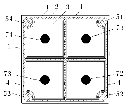
[0032] See attached figure 1 . A network electrode suitable for high-power GaN-based LED chips, using a chip with a size of 1mm×1mm. First, grooves 2 are etched on the front of the GaN epitaxial layer until the N layer, and the chip is divided into 4 mesas 1 : The line width of the mesa 1 is 100 microns, and the line width of the trench 2 is 30 microns; the mesa 1 is a rectangular structure, and its length and width are 762 microns. The trench 2 completely disconnects the quantum well layer, the superlattice layer, and the P-type GaN layer on the N-type layer of the four mesas 1 . Metal electrodes are deposited in the trench 2 and on the mesa 1, and the metal line width in the trench 2 and on the mesa 1 is 20 microns.

[0033] The N-type electrode is a network formed by the first N-type metal pad 51, the second N-type metal pad 52, the third N-type metal pad 53, the fourth N-type metal pad 54 and the N-type metal electrode 4. The N-type metal electrode 4 is a strip electrod...

Embodiment 2

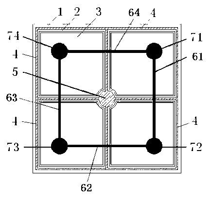
[0038] See attached figure 2 . A network electrode suitable for high-power GaN-based LED chips, using a chip with a size of 762 microns × 762 microns. First, grooves 2 are etched on the front of the GaN epitaxial layer until the N layer, and the chip is divided into 4 mesas. 1: The line width of trench 2 is 23 microns, and the line width of mesa 1 is 76 microns. The groove 2 completely disconnects the quantum well layer, the superlattice layer, and the P-type GaN layer on the N-type layer of the four mesas 1 . Metal electrodes are deposited in the trench 2 and on the mesa 1, and the metal line width in the trench 2 and on the mesa 1 is 15 microns.

[0039] The N-type electrode is a network electrode composed of N-type metal pads 5 and N-type metal electrodes 4. The N-type metal electrodes 4 are strip-shaped electrodes interlaced to form a network, and are arranged on the mesa structure of the mesa 1. Buried by a silicon dioxide passivation layer and isolated from the edge ...

Embodiment 3

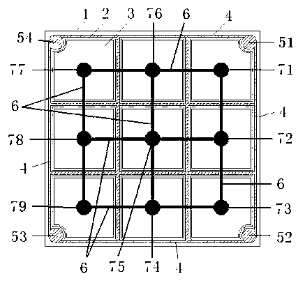
[0044] See attached image 3 . A network electrode suitable for high-power GaN-based LED chips, using a chip with a size of 1500 microns × 1500 microns. First, grooves 2 are etched on the front of the GaN epitaxial layer until the N layer, and the chip is divided into 9 mesas. 1: The line width of trench 2 is 45 microns, and the line width of mesa 1 is 150 microns. The groove 2 completely disconnects the quantum well layer, the superlattice layer, and the P-type GaN layer on the N-type layer of the nine mesas 1 . Metal electrodes are deposited in the trench 2 and on the mesa 1, and the metal line width in the trench 2 and on the mesa 1 is 30 microns.

[0045] The N-type electrode is a network formed by the first N-type metal pad 51, the second N-type metal pad 52, the third N-type metal pad 53, the fourth N-type metal pad 54 and the N-type metal electrode 4. The N-type metal electrode 4 is a strip-shaped electrode interlaced to form a network, which is arranged on the mesa ...


PUM


Abstract

The invention relates to the technical field of semiconductor illumination and provides a network-shaped electrode applicable to high-power GaN-based LED chips. Each electrode of a chip is composed of a network-shaped electrode and metal pads, the adopted electrodes at least have center inversion symmetry, secondary axial symmetry and quartic axial symmetry, wherein the secondary axial symmetry and the quartic axial symmetry are achieved by surrounding and being perpendicular to the center normal of the chip, and accordingly the electrodes can coincide when the chip rotates by 180 degrees, 270 degrees and 360 degrees around the center normal. A portion above an N-type GaN layer in an epitaxial layer is divided into multiple independent units not contacting with one another by the aid of N-type electrode slots on a projection plane perpendicular to the chip central axis, so that the units are unaffected by one another. Current distribution is more even by more electrode symmetry elements, and uneven heating of the chip is improved effectively. P-type metal pads and N-type metal pads can be selectively connected during routing by the aid of high symmetry of the P-type metal pads and the N-type metal pads, and accordingly flexibility of routing is improved.

Description

technical field [0001] The invention relates to the technical field of semiconductor lighting, in particular to a network electrode suitable for high-power GaN-based LED chips, which has uniform current distribution and better photoelectric characteristics. Background technique [0002] LED is a new generation of solid-state light source. It has many advantages such as small size, low power consumption, long service life, high luminous efficiency, low heat, environmental protection and energy saving, and durability, so it has a broad application market. At present, LED has been widely used in backlight, traffic lights, large-screen display, automotive lighting, decorative lighting and other fields. With the continuous maturity and development of GaN-based LED technology, lighting fixtures based on GaN-based high-power LED chips are expected to become the fourth generation of lighting sources and have extremely broad application prospects. [0003] At present, commercial GaN...

Claims


Application Information

Patent Timeline
Patent Type & Authority Applications(China)
IPC IPC(8): H01L33/38
Inventor 杨旅云张国龙曹凤凯刘献伟张宇欣赵明田光磊吴东平陈晓鹏常志伟李浩
Owner 施科特光电材料(昆山)有限公司
Why Eureka
Try Eureka