Atomic force microscope imaging method and device of microscopic monitoring type selectable region

A technology of atomic force microscopy and atomic force microscopy, which is applied in measuring devices, scanning probe microscopy, instruments, etc., can solve the problems of randomness and blindness, limitations of microscopic imaging performance, scanning imaging, etc., and achieve improved Operational performance and scanning imaging quality, real-time monitoring and area selection, and the effect of improving efficiency and reliability

Inactive Publication Date: 2012-10-10
ZHEJIANG UNIV
View PDF7 Cites 14 Cited by
  • Summary
  • Abstract
  • Description
  • Claims
  • Application Information

AI Technical Summary

Problems solved by technology

[0003] It should be pointed out that most AFM technologies and instruments at home and abroad (hereinafter also referred to as conventional or ordinary AFM), although their scanning detection accuracy can reach the nanometer level, there are also complex operations, strict maintenance requirements, and selection of scanning areas. Disadvantages such as randomness and blindness, limitations in microscopic imaging performance, etc.
For example, since the size of the microcantilever of AFM is very small, the total length is generally 100 μm or 200 μm, and the size of the tip of the microcantilever is generally on the order of microns. The tip of the micro-cantilever is aligned, and the quality of adjustments such as the focus and alignment of the laser spot directly affects the quality of AFM scanning imaging; similarly, in the absence of microscopic monitoring, AFM can only randomly use the micro-cantilever ( Microprobe) scans and images the surface area of ​​the sample facing the microprobe, so there is randomness and blindness; in addition, it is impossible to perform selection and AFM scanning imaging on the sample surface area of ​​interest

Method used


Image

  • Atomic force microscope imaging method and device of microscopic monitoring type selectable region
  • Atomic force microscope imaging method and device of microscopic monitoring type selectable region

Examples


Embodiment Construction

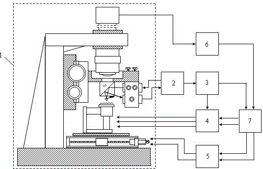
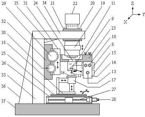
[0013] Micro-monitoring type optional area AFM imaging method: using the method of combining optical micro-monitoring with AFM micro-imaging, and combining the AFM scanner with a two-dimensional stepping The transflective prism, optical microscope objective lens and CCD are used for real-time microscopic monitoring of the atomic force microscope scanning area of ​​the sample; at the same time, the adjustment and alignment process of the laser beam on the atomic force microscope microprobe is monitored, so as to effectively Improve the operational performance and scanning imaging quality of the atomic force microscope; in addition, monitor the micro-nano approach process between the sample and the atomic force microscope microprobe, thereby improving the efficiency and reliability of the micro-nano approach operation; introduce a two-dimensional stepping and micro-moving stage, Under microscopic monitoring, select the area of ​​the sample surface of interest, and cooperate with ...


PUM


Abstract

The invention discloses an atomic force microscope imaging method and an atomic force microscope (AFM) imaging device of a microscopic monitoring type selectable region. Microscopic monitoring and selectable region AFM imaging of an AFM scanning region are realized by using a method for combining optical microscopic monitoring with AFM microscopic imaging and combining an AFM scanner and a two-dimensional step micropositioner. The device is provided with an AFM probe and an AFM imaging and control system, wherein the AFM probe comprises a laser device, a semi-transparent semi-reflective prism, a microprobe, a position sensitive element, a sample, a sample table, a scanner, a microscope objective, a CCD (Charge Coupled Device), a two-dimensional step micropositioner and the like; and the AFM imaging and control system comprises a preamplifier, an XY scanning and Z feedback control unit, an XYZ high-voltage amplifying module, a step control module, a video acquisition module, a computer, a hardware interface and the like. The method and the device have the advantages that real-time monitoring and region selection of a micro / nano sample scanning region are realized, adjustment and alignment of an optical path and an approximation process of the sample and the microprobe can be monitored, and the randomness, the blindness and the limitation of the conventional AFM technologies in the aspects are overcome.

Description

technical field [0001] The invention relates to a microscopic monitoring type optional area atomic force microscopic imaging method and device. Background technique [0002] Micro-nano technology is a high-tech field that has developed rapidly in the world in recent years. Developed countries such as the United States, Europe, and Japan, as well as my country, have included micro-nano technology as a priority frontier technology field in the national science and technology development strategy in the 21st century. The scanning probe microscope (SPM) family, represented by scanning tunneling microscope (STM) and atomic force microscope (AFM), is a widely used micro-nano detection technology and instrument in the field of micro-nano technology, and is an important part of the development of micro-nano technology. one of the foundations. Among them, AFM is not limited by the conductivity (conductor, semiconductor and insulator), magnetism (magnet and non-magnet) and material s...

Claims


Application Information

Patent Timeline
Patent Type & Authority Applications(China)
IPC IPC(8): G01Q60/24
Inventor 章海军丑若帆张冬仙刘明月
Owner ZHEJIANG UNIV
Why Eureka
Try Eureka