
Process for forming an epitaxial layer

An epitaxial layer and process technology, applied in the field of microelectronics, can solve the problems of difficult realization and expensive hard mask, and achieve the effect of simplifying control

Inactive Publication Date: 2012-10-17
STMICROELECTRONICS CROLLES 2 +1
View PDF3 Cites 0 Cited by
  • Summary
  • Abstract
  • Description
  • Claims
  • Application Information

AI Technical Summary

Problems solved by technology

[0008] Even so, using a hard mask is expensive and difficult to implement

Method used


Image

  • Process for forming an epitaxial layer
  • Process for forming an epitaxial layer
  • Process for forming an epitaxial layer

Examples


Embodiment Construction

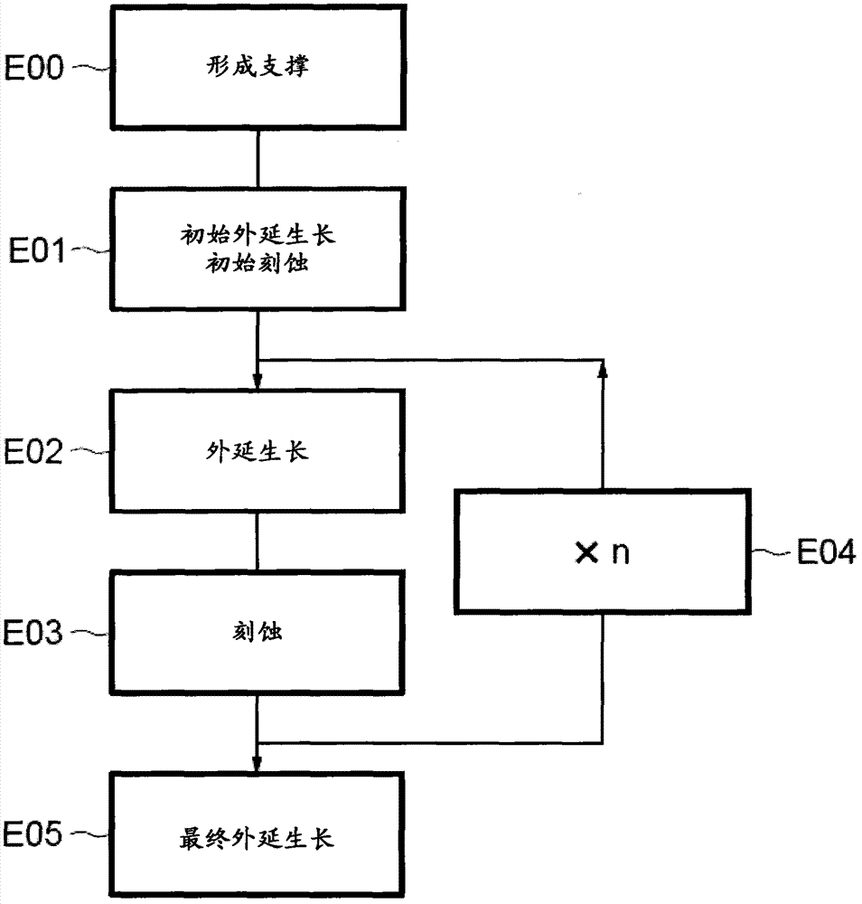
[0037] figure 1 The steps of the process according to one aspect of the present invention are schematically described.

[0038] In the first step E00, a support is formed, and it is desirable to form an epitaxial layer on the support. This step E00 may include forming a semiconductor substrate or a silicon-on-insulator (SOI) substrate, and forming at least an initial single crystal structure and an initial polycrystalline structure. The single crystal structure may be contained in a support, such as an SOI substrate. The polycrystalline structure may be an insulated gate region fabricated on the substrate or part of the initial single crystal structure.

[0039] Of course, the formation of the support may include forming other components in semiconductor materials other than silicon.

[0040] Then, step E01 of initial epitaxial growth of the initial material and initial etching is optionally performed.

[0041] Step E01 is particularly applicable to the thinnest (for example, thickn...


PUM


Abstract

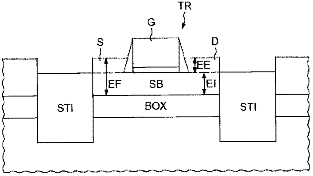
The invention relates to a process for forming an epitaxial layer, especially to a process, comprising the steps that a layer of a semiconductor material is epitaxially grown on a single-crystal semiconductor structure (S, D) and on a polycrystalline semiconductor structure (G). The epitaxial layer is then etched in order to preserve a non-zero thickness of said material on the single-crystal structure(S, D) and a zero thickness on the polycrystalline structure. The process of growth and etch is repeated, with the same material or with a different material in each repetition, until a stack of epitaxial layers on said single-crystal structure (S, D) has reached a desired thickness (EE).

Description

Technical field [0001] The present invention relates to microelectronics, and particularly to the formation of epitaxial layers of semiconductor materials, especially the formation of source and drain regions of transistors such as fully depleted transistors fabricated on silicon-on-insulator (SOI) substrates The epitaxial layer. Background technique [0002] The epitaxial growth step can be used to control the electrical characteristics of the source and drain regions of the insulated gate transistor. The level of dopants present in these single crystal regions can be specifically controlled by introducing dopants into the epitaxial silicon layer. It is also possible to introduce germanium atoms or carbon atoms in order to modify the mechanical strain in the epitaxial layer and in order to increase the mobility of charge carriers in the source and drain regions. [0003] In addition, traditionally, the gate of a transistor includes at least one polysilicon layer that may be depo...

Claims


Application Information

Patent Timeline
IPC IPC(8): H01L21/336H01L21/20
CPCH01L29/0873H01L29/78H01L21/0262H01L29/7848H01L21/02532H01L21/02636H01L29/66628H01L29/0856H01L21/02381
Inventor D·迪塔特Y·康皮德利D·佩利谢尔-塔农N·卢贝
Owner STMICROELECTRONICS CROLLES 2
Learn More