Manufacturing method of thin film transistor and manufacturing method of array base plate

A technology for thin film transistors and a manufacturing method, which is applied to the manufacture of array substrates and the manufacture of thin film transistors, can solve problems such as low alignment accuracy, uneven capacitance, alignment shift, etc., and achieve the effect of improving product quality

Active Publication Date: 2012-10-17
BOE TECH GRP CO LTD
View PDF4 Cites 20 Cited by
  • Summary
  • Abstract
  • Description
  • Claims
  • Application Information

AI Technical Summary

Problems solved by technology

[0003] In the existing method of manufacturing TFT-LCD, the source and drain of the thin film transistor are fully aligned with the alignment marks on each corner of the surface. This alignment method has low alignment accuracy and will cause gate There is an alignment offset between the source, the gate and the drain, resulting in uneven capacitance between the source / drain and the gate, which in turn leads to uneven chromaticity of the LCD display and affects product quality

Method used


Image

  • Manufacturing method of thin film transistor and manufacturing method of array base plate
  • Manufacturing method of thin film transistor and manufacturing method of array base plate
  • Manufacturing method of thin film transistor and manufacturing method of array base plate

Examples


Embodiment Construction

[0024] The following will clearly and completely describe the technical solutions in the embodiments of the present invention with reference to the accompanying drawings in the embodiments of the present invention. Obviously, the described embodiments are only some, not all, embodiments of the present invention. Based on the embodiments of the present invention, all other embodiments obtained by persons of ordinary skill in the art without making creative efforts belong to the protection scope of the present invention.

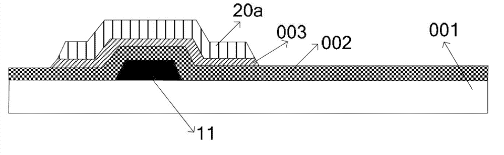
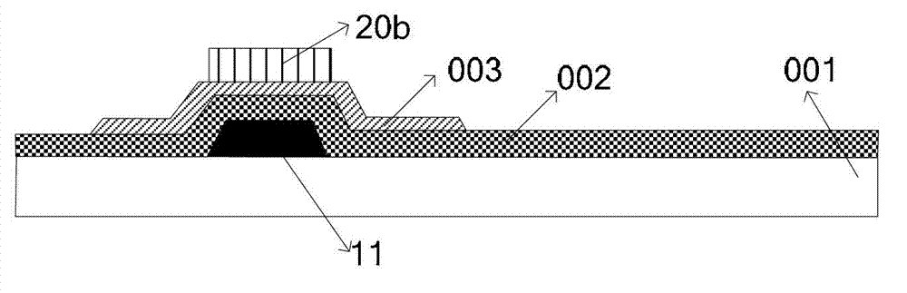
[0025] refer to Figure 1-Figure 6 , the manufacturing method of the thin film transistor provided by the embodiment of the present invention, comprises the following steps:

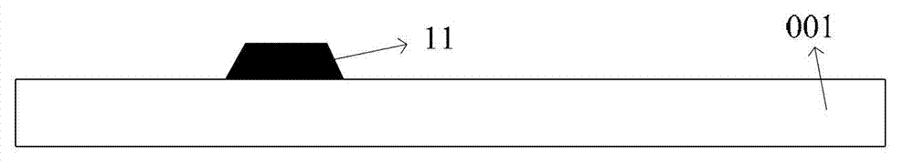
[0026] S11, such as figure 1 As shown, a gate 11 is formed on a transparent substrate 001 .

[0027] Exemplarily, a gate metal thin film may be deposited on a transparent substrate by using a magnetron sputtering device, and a patterning process may be used to form a gate. Wherein, t...


PUM


Abstract

The embodiment of the invention provides a manufacturing method of a thin film transistor and a manufacturing method of an array base plate, relates to the filed of liquid crystal panel manufacturing and enables a source/drain and a grid to be exactly aligned. The manufacturing method of the thin film transistor comprises the following steps of: forming a grid on a transparent base plate; forming a grid insulating layer on the base plate with the grid; manufacturing a transparent semiconductor thin film on the grid insulating layer, forming a semiconductor layer through using a picture composition technique, and reserving a photoresist above the semiconductor layer; carrying out exposure treatment on the reserved photoresist by taking the grid as a mask from one side of the transparent base plate, and forming a channel photoresist corresponding to the grid after developing; and manufacturing a source-drain metal thin film on the base plate with the channel photoresist, peeling off the channel photoresist and the source-drain metal thin film on the channel photoresist, and forming the source and the drain by using the picture composition technique. The two methods are applied to manufacturing products or devices including thin film transistors.

Description

technical field [0001] The invention relates to the field of manufacturing liquid crystal panels, in particular to a method for manufacturing a thin film transistor and a method for manufacturing an array substrate. Background technique [0002] Thin Film Transistor Liquid Crystal Display (TFT-LCD for short) has the advantages of small size, low power consumption, and no radiation, and occupies a dominant position in the current flat panel display market. [0003] In the existing method of manufacturing TFT-LCD, the source and drain of the thin film transistor are fully aligned with the alignment marks on each corner of the surface, and the alignment accuracy of this alignment method is not high, which will cause gate There is an alignment offset between the source, the gate and the drain, resulting in uneven capacitance between the source / drain and the gate, which in turn leads to uneven chromaticity of the liquid crystal display and affects product quality. Contents of t...

Claims


Application Information

Patent Timeline
Patent Type & Authority Applications(China)
IPC IPC(8): H01L21/336H01L21/77G02F1/1362G02F1/1368
CPCH01L29/66765H01L29/4908G02F1/1362H01L27/1259H01L29/458G02F1/136231
Inventor 高涛宁策于航张方振
Owner BOE TECH GRP CO LTD
Why Eureka
Try Eureka