

Semiconductor packaging structure for stacking and manufacturing method thereof
A manufacturing method and semiconductor technology, applied in the direction of semiconductor/solid-state device manufacturing, semiconductor devices, semiconductor/solid-state device components, etc.
- Summary
- Abstract
- Description
- Claims
- Application Information
AI Technical Summary
Problems solved by technology
Method used
Image

Examples
Embodiment Construction
[0018] The following descriptions of the various embodiments refer to the accompanying drawings to illustrate specific embodiments in which the present invention can be practiced. Furthermore, the directional terms mentioned in the present invention, such as "up", "down", "front", "back", "left", "right", "inside", "outside" or "side", etc., It is only for orientation with reference to the attached drawings. Therefore, the directional terms used are used to illustrate and understand the present invention, but not to limit the present invention.
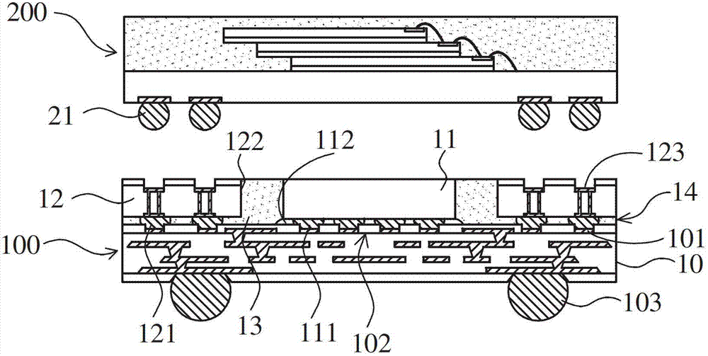
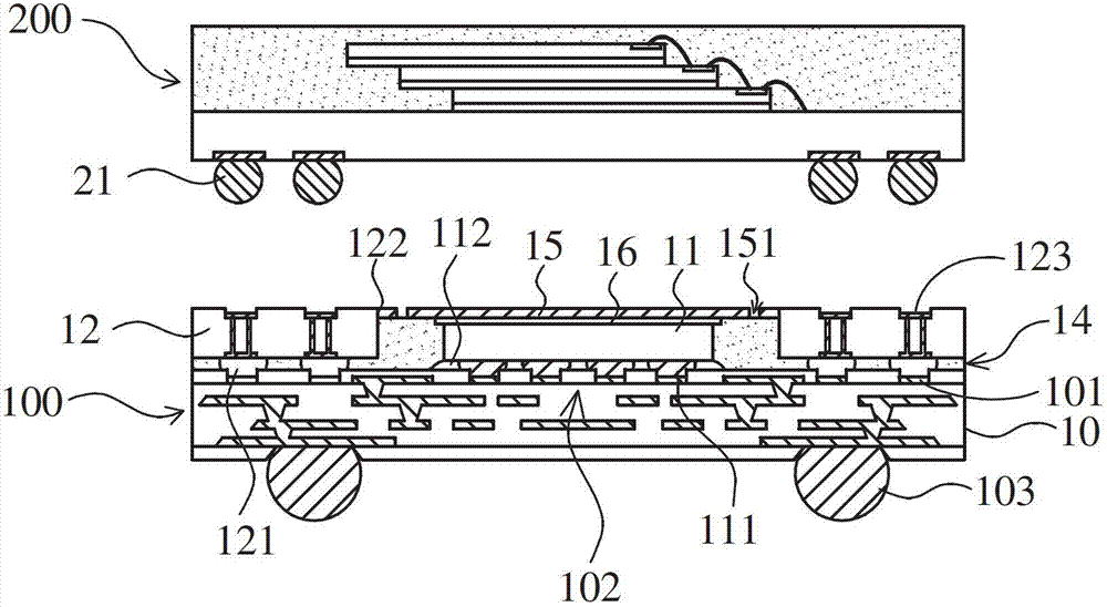
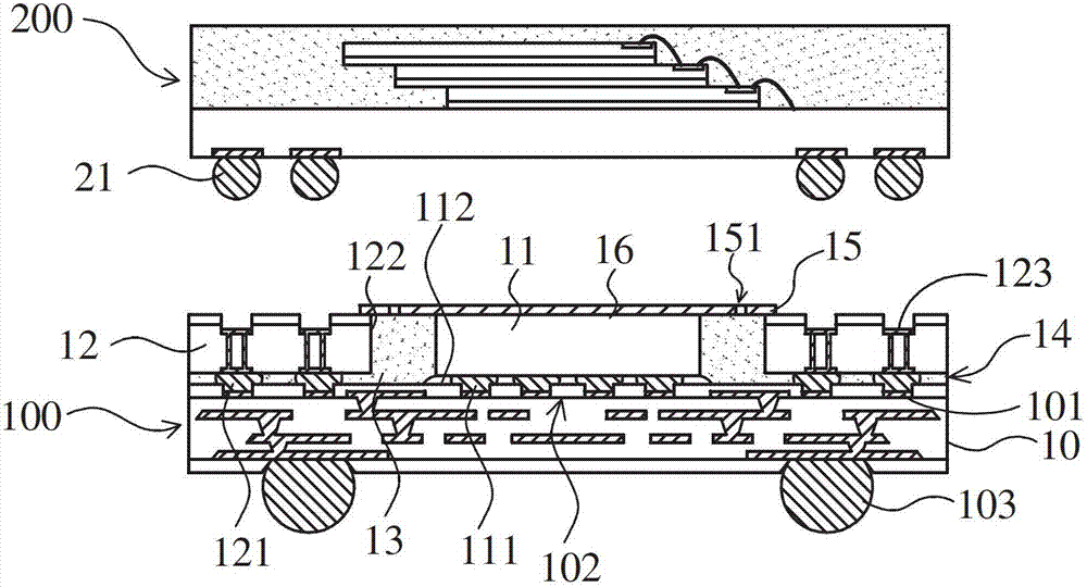
[0019] Please refer to figure 1 As shown, the semiconductor package structure for stacking according to the first embodiment of the present invention is mainly applied to the lower package 100 as a stacked package (POP), and is used to combine an upper package 200. Hereinafter, the The stacked semiconductor package structure is directly referred to as the lower package 100 . In this embodiment, the lower package body 100 includes: ...
PUM
 Abstract
Description
Claims
Application Information