Gallium nitride device structure and preparation method thereof

A device structure, gallium nitride technology, applied in electric solid state devices, semiconductor devices, semiconductor/solid state device components, etc., can solve problems such as high cost and poor heat dissipation effect, and achieve improved yield, thickness uniformity and flatness The effect of low degree requirements and cost reduction

Pending Publication Date: 2017-08-11
母凤文 +1
View PDF3 Cites 10 Cited by
  • Summary
  • Abstract
  • Description
  • Claims
  • Application Information

AI Technical Summary

Problems solved by technology

[0007] In view of this, the present invention provides a gallium nitride device structure with high heat dissipation performance and its preparation method to solve the problems of high cost and poor heat dissipation effect of gallium nitride heat dissipation solutions in the prior art

Method used


Image

  • Gallium nitride device structure and preparation method thereof
  • Gallium nitride device structure and preparation method thereof
  • Gallium nitride device structure and preparation method thereof

Examples


Embodiment Construction

[0049] In order to make the object, technical solution and advantages of the present invention clearer, the present invention will be described in further detail below in conjunction with specific embodiments and with reference to the accompanying drawings. The specific embodiments and drawings are only used to better understand the content of the present invention, but not to limit the protection scope of the present invention. The components in the structures in the drawings of the embodiments are not scaled according to the normal scale, so they do not represent the actual relative sizes of the structures in the embodiments.

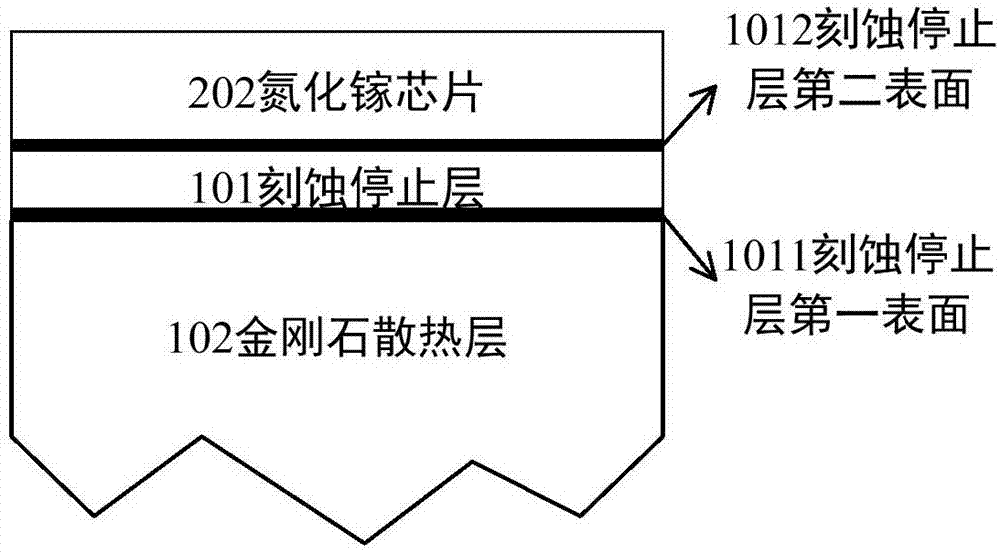
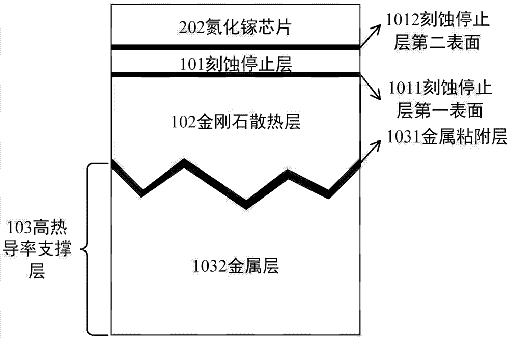
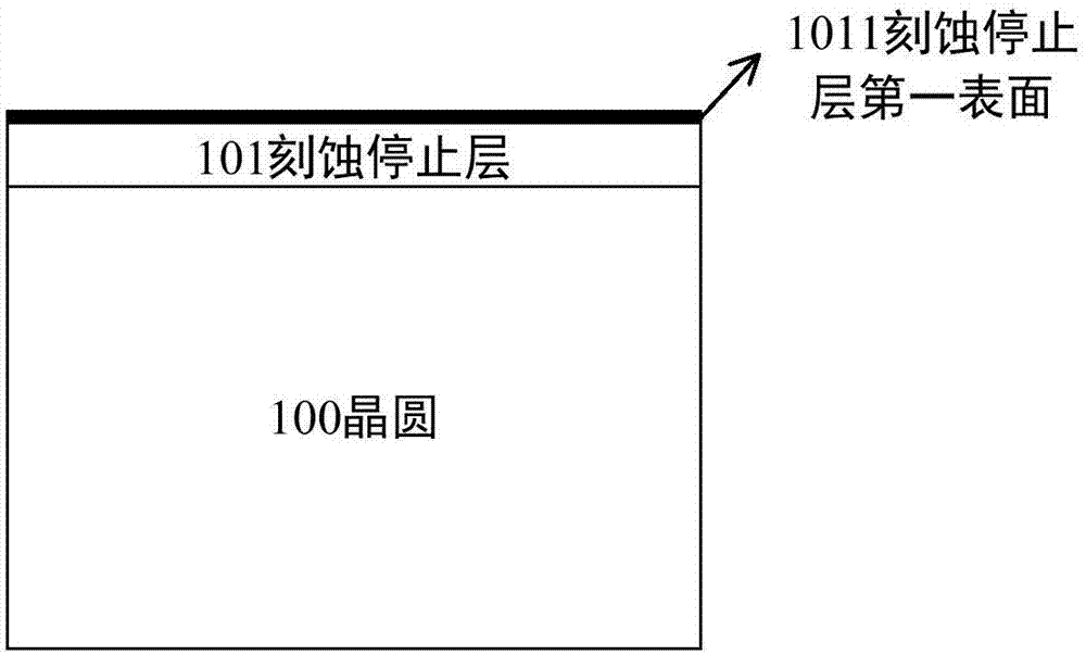
[0050] Such as Figure 1 to Figure 4 As shown, the gallium nitride device structure with high heat dissipation performance provided by the present invention is a layered structure, including a gallium nitride chip 202, an etch stop layer 101 and a diamond heat dissipation layer 102, wherein the etch stop layer 101 It has a first surface 1011 and a se...


PUM

PropertyMeasurementUnit
thicknessaaaaaaaaaa
thicknessaaaaaaaaaa
thicknessaaaaaaaaaa

Abstract

The invention discloses a gallium nitride device structure having high heat dissipation performance and a preparation method thereof. The gallium nitride device structure comprises a gallium nitride chip, an etching stopping layer, and a diamond heat dissipation layer. The etching stopping layer is provided with a first surface, which is used as a growth interface, and the diamond heat dissipation layer is grown on the first surface of the etching stopping layer. The etching stopping layer is provided with a second surface, which is opposite to the first surface, and is used as a bonding interface, and the gallium nitride chip is disposed on the second surface of the etching stopping layer in a bonding way. The etching stopping layer is formed by adopting a high thermal conductivity material. The production method of the gallium nitride chip and diamond bonding structure adopts a low temperature technology, and a warping problem caused by thermal expansion mismatch under high temperature is prevented, and no damages on existing devices are caused, and therefore integration between the gallium nitride wafer or chip provided with the device and a thin diamond layer is realized, a self-supporting diamond thick film substrate is not required, enhancement of heat dissipation performance is guaranteed, and at the same time, costs are obviously reduced, and then problems of a gallium nitride heat dissipation scheme such as high costs and poor heat dissipation effect are solved.

Description

technical field [0001] The invention relates to the technical fields of semiconductor technology and semiconductor packaging, in particular to a gallium nitride device structure with high heat dissipation performance and a preparation method thereof. Background technique [0002] Gallium nitride has the advantages of large band gap, direct band gap, fast electron drift, high temperature resistance, etc., and is suitable for the preparation of high-power, high-frequency electronic and optoelectronic devices, such as microwave transistors. The heat dissipation of high-power and high-frequency GaN devices is a key factor affecting device reliability and life. One of the current methods to solve the heat dissipation problem of GaN devices is to integrate GaN with diamond with high thermal conductivity. The integration methods mainly include: [0003] (1) Growth of gallium nitride on diamond. This method is to epitaxially grow the required gallium nitride layer on single crysta...

Claims


Application Information

Patent Timeline
Patent Type & Authority Applications(China)
IPC IPC(8): H01L23/373H01L29/20
CPCH01L29/2003H01L23/3735
Inventor 母凤文赫然
Owner 母凤文
Why Eureka
Try Eureka