SiGe base vertical channel strain BiCMOS (Bipolar Complementary Metal Oxide Semiconductor) integrated device and manufacturing method

A vertical channel, integrated device technology, used in semiconductor/solid-state device manufacturing, electrical solid-state devices, semiconductor devices, etc., can solve the increase in device feature size integration and complexity, and do not have the conditions and limitations to replace silicon-based processes Problems such as the development of Si integrated circuit manufacturing process

Inactive Publication Date: 2012-10-17
XIDIAN UNIV
View PDF8 Cites 3 Cited by
  • Summary
  • Abstract
  • Description
  • Claims
  • Application Information

AI Technical Summary

Problems solved by technology

However, with the further increase of the scale of integrated circuits, the reduction of device feature size, the increase of integration and complexity, especially after the device feature size enters the nanometer scale, the limitations of materials and physical characteristics of SiCMOS devices have gradually emerg

Method used


Image

  • SiGe base vertical channel strain BiCMOS (Bipolar Complementary Metal Oxide Semiconductor) integrated device and manufacturing method

Examples


Embodiment 1

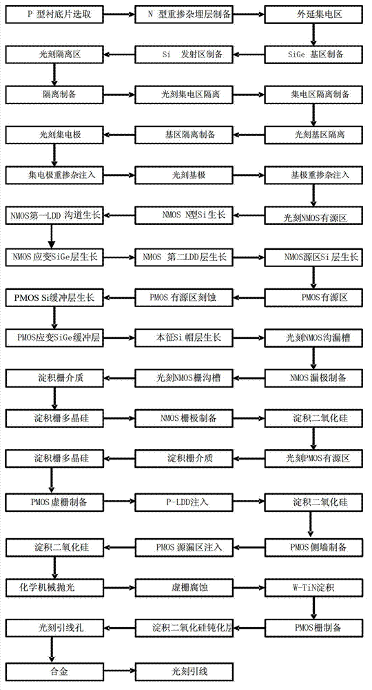
[0133] Embodiment 1: The SiGe-based vertical channel strained BiCMOS integrated device and circuit with a conductive channel of 45nm are prepared, and the specific steps are as follows:

[0134] Step 1, preparation of the buried layer.

[0135] (1a) Select the doping concentration to be 5×10 14 cm -3 A P-type Si sheet as a substrate;

[0136] (1b) Thermally oxidize a layer of SiO with a thickness of 300nm on the substrate surface 2 layer;

[0137] (1c) Photoetching the buried layer region, implanting N-type impurities into the buried layer region, and annealing at 800° C. for 90 minutes to activate the impurities to form an N-type heavily doped buried layer region.

[0138] Step 2, preparing the active region of the bipolar device.

[0139] (2a) An N-type epitaxial Si layer with a thickness of 2 μm is epitaxially grown on the substrate as the collector region, and the doping concentration of this layer is 1×10 16 cm -3 ;

[0140] (2b) Using chemical vapor deposition (C...

Embodiment 2

[0212] Embodiment 2: The conductive channel is prepared as a SiGe-based vertical channel strained BiCMOS integrated device and circuit, and the specific steps are as follows:

[0213] Step 1, preparation of the buried layer.

[0214] (1a) Select the doping concentration to be 1×10 15 cm -3 A P-type Si sheet as a substrate;

[0215] (1b) Thermally oxidize a layer of SiO with a thickness of 400nm on the substrate surface 2 layer;

[0216] (1c) Photoetching the buried layer region, implanting N-type impurities into the buried layer region, and annealing at 900° C. for 60 minutes to activate the impurities to form an N-type heavily doped buried layer region.

[0217] Step 2, preparing the active region of the bipolar device.

[0218] (2a) An N-type epitaxial Si layer with a thickness of 2.5 μm is epitaxially grown on the substrate as a collector region, and the doping concentration of this layer is 5×10 16 cm -3 ;

[0219] (2d) Using chemical vapor deposition (CVD), grow a l...

Embodiment 3

[0291] Embodiment 3: The SiGe-based vertical channel strained BiCMOS integrated device and circuit with a conductive channel of 22nm are prepared, and the specific steps are as follows:

[0292] Step 1, preparation of the buried layer.

[0293] (1a) Select the doping concentration to be 5×10 15 cm -3 A P-type Si sheet as a substrate;

[0294] (1b) Thermally oxidize a layer of SiO with a thickness of 500nm on the surface of the substrate 2 layer;

[0295] (1c) Photoetching the buried layer region, implanting N-type impurities into the buried layer region, and annealing at 950° C. for 30 minutes to activate the impurities to form an N-type heavily doped buried layer region.

[0296] Step 2, preparing the active region of the bipolar device.

[0297] (2a) An N-type epitaxial Si layer with a thickness of 3 μm is epitaxially grown on the substrate as the collector region, and the doping concentration of this layer is 1×10 17 cm -3 ;

[0298] (2d) Using chemical vapor deposi...


PUM

PropertyMeasurementUnit
Thicknessaaaaaaaaaa
Thicknessaaaaaaaaaa
Thicknessaaaaaaaaaa

Abstract

The invention discloses a SiGe base vertical channel strain BiCMOS (Bipolar Complementary Metal Oxide Semiconductor) integrated device and a manufacturing method. The method comprises the following steps of: manufacturing a SiGe HBT (Heterojunction Vipolar Transistor) device at a bipolar device area on a Si substrate sheet; etching an active area of an NMOS (N-Channel Metal Oxide Semiconductor) device; extensionally growing five layers of materials at the area so as to form the active area of the NMOS device; manufacturing the NMOS device; etching an active area of the PMOS (P-Channel Metal Oxide Semiconductor) device; extensionally growing three layers of materials at the area so as to form the active area of the PMOS device; forming a virtual grid and accomplishing the manufacturing of the PMOS device; and forming the SiGe base vertical channel strain BiCMOS integrated device and a circuit. The characteristics that the electronic mobility rate at the vertical direction and the hole mobility rate at the horizontal direction of the SiGe material are higher than that of the relaxation Si are utilized; and through a low temperature process, a circuit of the performance-enhanced SiGe base vertical channel strain BiCMOS integrated device is manufactured.

Description

technical field [0001] The invention belongs to the technical field of semiconductor integrated circuits, and in particular relates to a SiGe-based vertical channel strained BiCMOS integrated device and a preparation method. Background technique [0002] Semiconductor integrated circuits are the foundation of the electronics industry, and people's huge demand for the electronics industry has prompted the rapid development of this field. In the past few decades, the rapid development of the electronics industry has had a huge impact on social development and national economy. At present, the electronics industry has become the largest industry in the world, occupying a large share in the global market, and its output value has exceeded 1 trillion US dollars. [0003] SiCMOS integrated circuits have the advantages of low power consumption, high integration, low noise and high reliability, and occupy a dominant position in the semiconductor integrated circuit industry. Howeve...

Claims


Application Information

Patent Timeline
IPC IPC(8): H01L27/06H01L21/8249
Inventor 宋建军张鹤鸣王海栋周春宇胡辉勇宣荣喜戴显英郝跃
Owner XIDIAN UNIV
Why Eureka
Try Eureka