Light-emitting element

A technology of light-emitting elements and light-emitting functional layers, which is applied in the direction of electrical components, semiconductor devices, circuits, etc., can solve the problems of uneven light emission, difficulty in luminous intensity, and difficulty in obtaining high luminous efficiency, and achieve high luminous efficiency and uniform luminous intensity. Effect

Active Publication Date: 2012-10-17
SANKEN ELECTRIC CO LTD
View PDF6 Cites 4 Cited by
  • Summary
  • Abstract
  • Description
  • Claims
  • Application Information

AI Technical Summary

Problems solved by technology

That is, even in the structure described in Patent Document 1, the elimination of unevenness in light emission due to uneven current is insufficient.
[0015] In the technology described in Patent Document 2, a plurality of p-side electrodes and n-side electrodes that are opaque to light are provided, so the luminous efficiency is greatly reduced
In addition, the current concentrates only in the narrow area sandwiched between the p-side electrode and the n-side electrode, so when observed locally, there is a problem of heat generation due to uneven light emission or current concentration.
[0016] That is, in a light-emitting element having a structure in which two electrodes are formed on one surface of the semiconductor light-emitting functional layer, it is difficult to obtain high luminous efficiency, and it is difficult to obtain uniform luminous intensity in the plane.

Method used


Image

  • Light-emitting element
  • Light-emitting element
  • Light-emitting element

Examples


no. 1 Embodiment approach

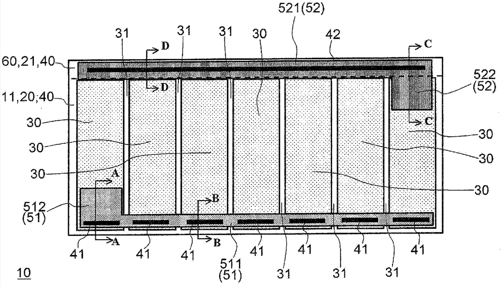
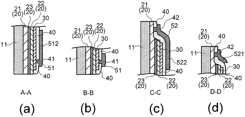
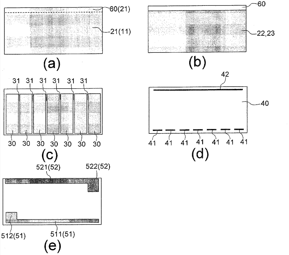
[0049] figure 1 It is a plan view seen from the upper surface side of the light emitting element 10 of the first embodiment. And, the sectional views of the A-A direction, B-B direction, C-C direction, and D-D direction in the plan view are respectively figure 2 (a) ~ (d). Furthermore, the n-type GaN layer (first semiconductor layer) 21, p-type GaN layer 22, transparent electrode 30, insulating layer 40, electrode The top view of (p-side electrode 51, n-side electrode 52) is image 3 (a) ~ (e). When looking down, the figure 1 Among them, the light-emitting element 10 has a rectangular shape long in the left-right direction.

[0050] The semiconductor light-emitting functional layer 20 that emits light in the light-emitting element 10 is formed on the substrate 11, and has an n-type GaN layer (the first semiconductor layer, hereinafter referred to as the n-type layer) 21, an MQW (Multi Quantum Well) layer 23 1. A stacked structure composed of a p-type GaN layer (second...

no. 2 Embodiment approach

[0075] Figure 7 It is a plan view seen from the upper surface side of the light emitting element 110 of the second embodiment. And, the sectional views of the E-E direction, the F-F direction, the G-G direction, the H-H direction, and the I-I direction in the plan view are respectively Figure 8 (a) ~ (e). Furthermore, the n-type layer 21, p-type layer 22, transparent electrode 30, insulating layer 40, electrodes (p-side electrode 51, n-side The top view of electrode 52) is Figure 9 (a) ~ (e). When viewed from above, the light emitting element 110 is Figure 7 A roughly square shape (1 side L) is shown.

[0076] The semiconductor light-emitting functional layer 20 that emits light in the light-emitting element 110 is formed on the substrate 11 as described above, and has a stacked structure composed of an n-type layer 21 , an MQW layer 23 , and a p-type layer 22 .

[0077] here, as Figure 9 As shown in (a), the n-type layer (first semiconductor layer) 21 on the subst...

no. 3 Embodiment approach

[0101] The light emitting element 210 of the third embodiment has a structure in which a light emitting diode having a structure similar to that of the light emitting element 10 of the first embodiment and a protective diode (diode) are monolithically connected on a substrate. Figure 11It is a circuit diagram of the light emitting element 210 of this structure. Here, the light emitting diode 220 and the protection diode 230 are reversely connected. In this case, when an excessive voltage is applied to the light emitting diode 220 , the protection diode 230 is turned on by the Zener effect to bypass the current, thereby protecting the light emitting diode 220 .

[0102] Figure 12 With figure 1 A plan view of the structure of the light emitting element 210 is similarly shown. and, Figure 13 (a) to (c) are cross-sectional views in the J-J direction, K-K direction, and L-L direction of the periphery of the protective diode portion in the light emitting element 210, respect...


PUM


Abstract

In a light-emitting element forming two electrodes on one surface of a semiconductor light-emitting function layer, high light-emitting efficiency is obtained, and uniform light-emitting strength is obtained in the surface. In the light-emitting element (10), (1) an n side contact opening (a first opening part) (42) and a p side contact opening (a second opening part) (41) are formed via respectively along two straight lines in parallel extension to two sides (an upper side, a lower side) oppositely disposed in a rectangle, (2) between the two straight lines, a plurality of gaps (transparent electrode opening parts (31)) between transparent electrodes (30) extending along the direction perpendicular to the two straight lines are formed, and therefore, uniformity of current without increase of light-shielding area is performed, and light-emitting uniformity is realized.

Description

technical field [0001] The present invention relates to the structure of a light-emitting element that emits light using a semiconductor as a constituent material. Background technique [0002] Semiconductor light emitting diodes (LEDs) are used for various purposes. For example, lighting equipment using light-emitting diodes has lower power consumption and lower heat generation than conventional incandescent bulbs and fluorescent lamps, so it is expected to replace incandescent bulbs and fluorescent lamps in the future. Here, the p-type semiconductor layer and the n-type semiconductor layer in the LED are generally formed by epitaxial growth, ion implantation, and the like. Therefore, a pn junction surface is formed parallel to the surface of the semiconductor wafer, and electrodes connected to the p side and electrodes connected to the n side are assigned to the upper and lower surfaces of the semiconductor layer. This light emitting element can be made to emit light by ...

Claims


Application Information

Patent Timeline
Patent Type & Authority Applications(China)
IPC IPC(8): H01L33/38H01L33/42
CPCH01L33/38H01L33/42
Inventor 杉森畅尚
Owner SANKEN ELECTRIC CO LTD
Why Eureka
Try Eureka