Device and method for machining large-area plane optical element

A technology of optical parts and processing devices, which is applied in the field of large-area planar optical parts processing devices, can solve the problems of low efficiency and high cost, and achieve the effects of reducing costs, reducing electrode temperature, and improving processing efficiency

Active Publication Date: 2012-10-24
HARBIN INST OF TECH
View PDF5 Cites 21 Cited by
  • Summary
  • Abstract
  • Description
  • Claims
  • Application Information

AI Technical Summary

Problems solved by technology

[0005] In order to solve the problems of high cost of the existing plasma polishing device and low efficiency of the existing plasm

Method used


Image

  • Device and method for machining large-area plane optical element
  • Device and method for machining large-area plane optical element
  • Device and method for machining large-area plane optical element

Examples


specific Embodiment approach 1

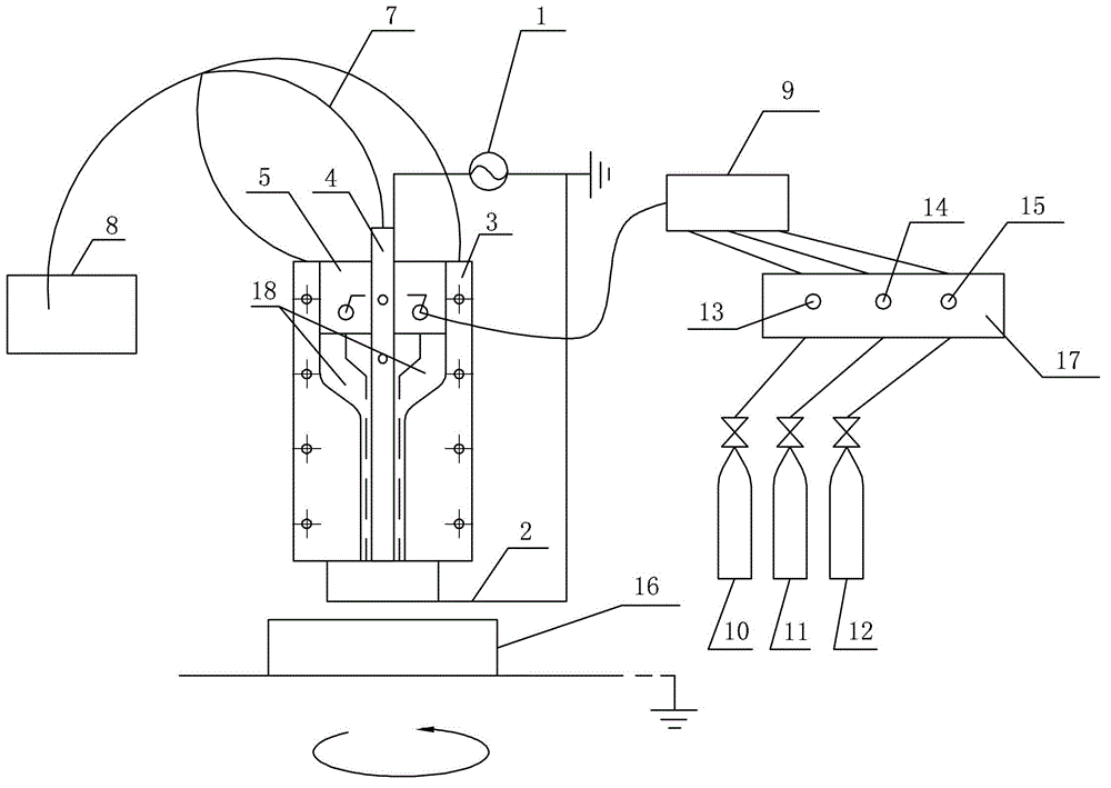
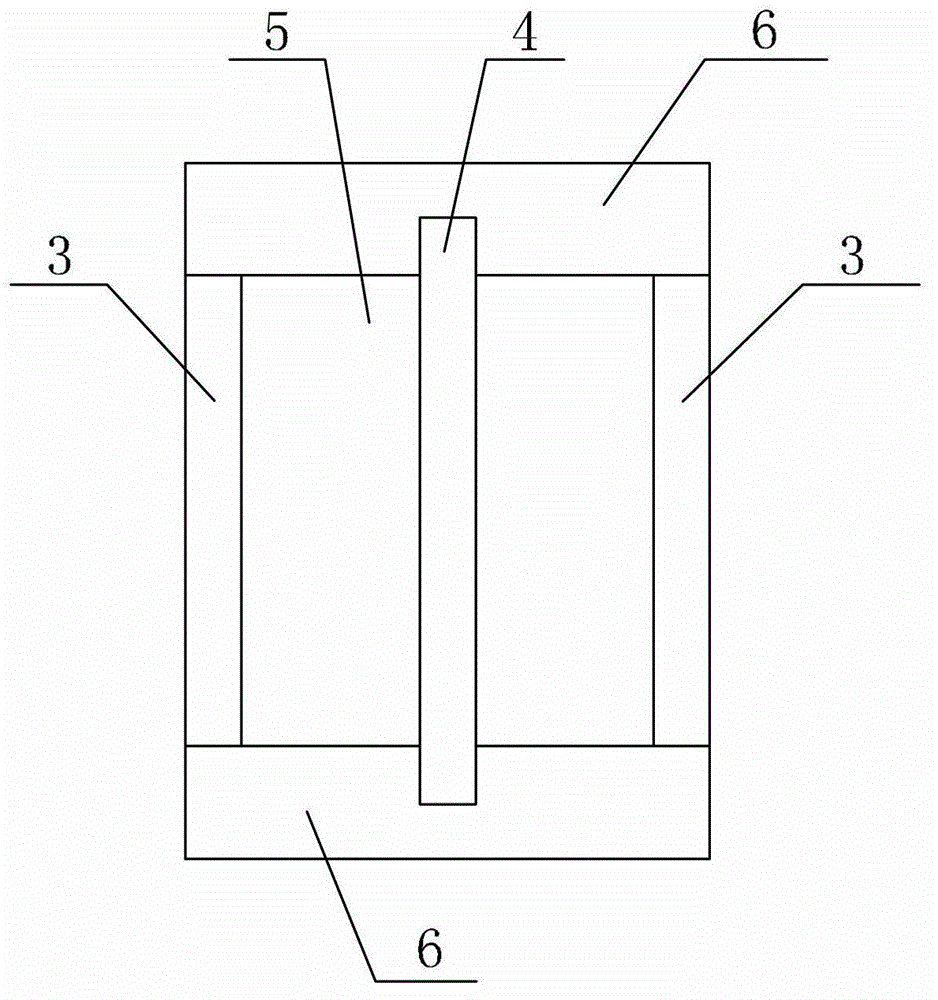
[0023] Specific implementation mode one: as Figure 1-5 As shown, the large-area planar optical part processing device of this embodiment includes a radio frequency power supply 1, a ground wire 2, an inner electrode 4, a deflector 5, a cooling pipe 7, a water tank 8, a flow controller 17, a helium cylinder 10, four Fluorocarbon bottle 11, oxygen bottle 12, two outer electrodes 3 and two isolation plates 6, the radio frequency power supply 1, ground wire 2, inner electrode 4, two outer electrodes 3 and two isolation plates 6 constitute plasma Flat plate discharge structure, the two external electrodes 3 are arranged symmetrically, and the two external electrodes 3 are opposite to the two isolation plates 6 to form a closed structure. The guide plate 5 is arranged on the upper part of the two external electrodes 3 Between the electrodes 3, the lower end of the inner electrode 4 passes through the deflector 5 and the inner electrode 4 is located between the two outer electrodes ...

specific Embodiment approach 2

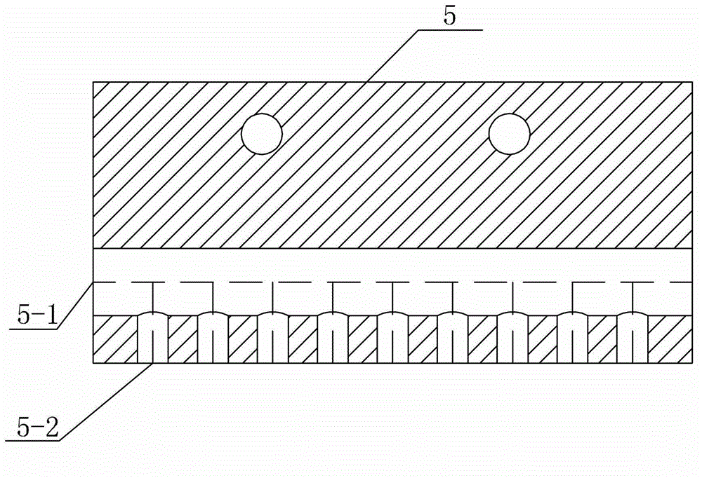
[0025] Specific implementation mode two: as Figure 4 As shown, the first cooling passage 4-1 in this embodiment is U-shaped. With such a design, the temperature of the internal electrodes can be reduced. Other components and connections are the same as those in the first embodiment.

specific Embodiment approach 3

[0026] Specific implementation mode three: as figure 1 As shown, the processing device in this embodiment further includes an air mixing valve 9, and the flow controller 17 communicates with the two first through holes 5-1 through the air mixing valve 9. With such a design, the gas in the flow controller 17 can be fully mixed. Other compositions and connections are the same as those in Embodiment 1 or 2.


PUM


Abstract

The invention discloses a device and a method for machining a large-area plane optical element, and relates to a device and a method for machining a plane optical element. With the adoption of the device and the method, the problems that the prior plasma polishing device is high in cost, and the polishing method is low in efficiency are solved. Two external electrodes and two isolating plates are opposite in pairs to form a closed structure; an internal electrode is located at the two external electrodes; two plasma generating cavities are formed among the two external electrodes, the two isolating plates and the internal electrode; and a helium tank, a carbon tetrafluoride bottle and an oxygen bottle are communicated with two first through holes through a flow controller. The method for machining the large-area plane optical element comprises the steps of adding cooling water to the electrodes, preheating the flow controller, controlling gas flow of helium and the carbon tetrafluoride by the flow controller, placing a workpiece to be machined on the electrodes on a working table so as to enable the workpiece to be machined to rotate counterclockwise, gradually increasing power on a radio frequency power source, controlling discharge of the stable plasma, turning off the radio frequency power source and a valve, and taking out the workpiece to be machined. The device and the method can be used for machining the large-area plane optical element.

Description

technical field [0001] The invention relates to a large-area plane optical part processing device and processing method. Background technique [0002] In recent years, there has been an increasing demand for large precision optical components. Traditional methods of processing optical components have resulted in surface damage and subsurface damage to optical components. Therefore, subsequent polishing, such as airbag polishing, chemical polishing, or magnetorheological polishing, is required. , the main problem of the above-mentioned polishing method is the long processing cycle, that is, the main problem faced by the finishing of large optical parts is low efficiency. [0003] Plasma chemical polishing is to make the reactive gas in an active plasma, which stimulates the chemical reaction. Plasma polishing is a non-contact polishing, which avoids surface and subsurface damage and has higher removal efficiency due to the chemical reaction. . [0004] Plasma chemical polis...

Claims


Application Information

Patent Timeline
IPC IPC(8): B24B1/00
Inventor 王波金会良李娜姚英学赵玺
Owner HARBIN INST OF TECH
Why Eureka
Try Eureka