Encapsulation substrate with embedded passive components and manufacturing method thereof

A technology of passive components and packaging substrates, applied in semiconductor/solid-state device manufacturing, printed circuits assembled with electrical components, printed circuits connected with non-printed electrical components, etc., can solve problems affecting wiring, long signal transmission paths, and electrical problems. Loss and other issues, to achieve the effect of not affecting the wiring, shortening the signal transmission path, and reducing the height

Active Publication Date: 2015-10-14
UNIMICRON TECH CORP
View PDF3 Cites 0 Cited by
  • Summary
  • Abstract
  • Description
  • Claims
  • Application Information

AI Technical Summary

Problems solved by technology

[0004] With the progress of science and technology, electronic devices are designed to be light, thin and short. However, the structure in which the passive components 12 are arranged on the substrate 10 in the prior art leads to an increase in the height of the overall packaging structure, which is not conducive to the thinness of the electronic device. Moreover, because the passive component 12 is arranged on the outer surface of the substrate 10, the signal transmission path between the inner circuit of the substrate 10 and the passive component is too long, which may easily lead to electrical loss and affect the electrical function.
In addition, because wiring is required on the surface of the substrate 10, the area where the passive components 12 can be placed is limited, resulting in a limited number of passive components 12. If it is necessary to add passive components 12, it will inevitably affect the wiring.

Method used


Image

  • Encapsulation substrate with embedded passive components and manufacturing method thereof
  • Encapsulation substrate with embedded passive components and manufacturing method thereof
  • Encapsulation substrate with embedded passive components and manufacturing method thereof

Examples


no. 1 example

[0062] see Figure 2A to Figure 2G , is a schematic cross-sectional view of the manufacturing method of the package substrate embedded with passive components of the present invention.

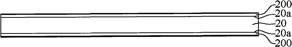
[0063] Such as Figure 2A As shown, firstly, a carrier board 20 is provided, and the two surfaces 20a of the carrier board 20 have a release film 200 and a metal layer 201 in sequence.

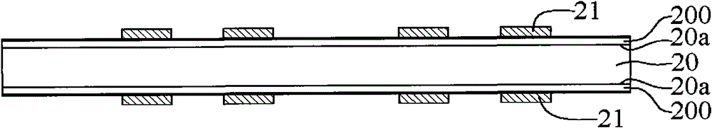
[0064] Such as Figure 2B As shown, next, a positioning pad 21 is formed on the metal layer 201 .

[0065] Such as Figure 2C As shown, the metal layer 201 on the two surfaces 20a of the carrier board 20 is covered with a first hot-melt dielectric layer 230; The pad 21 is used as a location, and then the passive component 22 is placed on the first heat-melt dielectric layer 230 . Wherein, the electrode pad 220 on the lower surface of the passive component 22 corresponds to the positioning pad 21 .

[0066] Such as Figure 2C' As shown, positioning pads 21' or 21" in different arrangements can also be fo...

no. 2 example

[0074] see Figure 3A to Figure 3G The main difference between this embodiment and the first embodiment is that the positioning pads are replaced by solder bumps, and the manufacturing steps for forming the dielectric layer unit and the second circuit layer are also different.

[0075] Such as Figure 3A As shown, provide as Figure 2A The carrier board 20 is used, and solder bumps 31 are formed on the metal layer 201 .

[0076] Such as Figure 3B As shown, provide as Figure 2C The passive component 22 , and the electrode pad 220 on the lower surface of the passive component 22 is connected to the solder bump 31 .

[0077] Such as Figure 3C As shown, a first heat-fusible dielectric layer 330 having an opening area 330a is provided on the metal layer 201 on the two surfaces 20a of the carrier board 20, so that the passive component 22 and the solder bump 31 are exposed on the metal layer 201. Opening area 330a.

[0078] Such as Figure 3D As shown, a core board 27 wit...

no. 3 example

[0084] see Figure 4A to Figure 4D The main difference between this embodiment and the first embodiment lies in the manufacturing steps of forming the first circuit layer and the build-up circuit structure.

[0085] Such as Figure 4A shown, continue Figure 2D manufacturing step, after forming the dielectric layer unit 23 by heating and pressing, the first circuit layer 44a is formed on the upper surface 23a of the dielectric layer unit 23, and the first circuit layer 44a and the upper surface of the passive component 22 There is a first conductive blind hole 440a electrically connected between the electrode pads 220; and a build-up circuit structure 45 is formed on the upper surface 23a of the dielectric layer unit 23 and the first circuit layer 44a. The build-up circuit structure 45 includes at least one dielectric layer 450 , a circuit layer 451 disposed on the dielectric layer 450 , and conductive blind vias 452 disposed in the dielectric layer 450 and electrically conn...


PUM


Abstract

The invention provides a packaging substrate of an embedded passive assembly. The packaging structure comprises a core board, a dielectric layer unit, a positioning pad, a passive assembly, a first line layer and a second line layer. The core board is provided with an opening, and the dielectric layer unit wraps the core board, full-fills the opening of the core board, and is provided with an upper surface and a lower surface. The positioning pad is embedded in the lower surface of the dielectric layer unit. The upper surface and lower surface of the passive assembly are provided with a plurality of electrode pads, and the passive assembly is embedded in the dielectric layer unit, arranged in the opening of the core board, and corresponds to the positioning pad. The first line layer is arranged on the upper surface of the dielectric layer unit, and a first conducting blind hole is electrically connected between the first line layer and the electrode pads arranged on the upper surface of the passive assembly. The second line layer is arranged on the lower surface of the dielectric layer unit, and a second conducting blind hole is electrically connected between the second line layer and the electrode pads arranged on the lower surface of the passive assembly. The passive assembly is embedded in the core board and the dielectric layer unit, thereby effectively lowering the height of the overall structure.

Description

technical field [0001] The invention relates to a packaging substrate and a manufacturing method thereof, in particular to a packaging substrate with passive components and a manufacturing method thereof. Background technique [0002] With the evolution of semiconductor packaging technology, the demand for passive components is also increasing; passive components do not affect the basic characteristics of the signal, but only pass the signal without changing the circuit components, generally refer to capacitors, resistors, inductors three. compared to active components. Since passive components cannot participate in electronic movement, when the voltage or current changes, its resistance and impedance will not change accordingly, so it needs to be connected with active components to operate. [0003] All kinds of products that need to be driven by electricity need to use passive components to achieve the function of electronic circuit control. The application range include...

Claims


Application Information

Patent Timeline
Patent Type & Authority Patents(China)
IPC IPC(8): H01L23/498H01L21/48H05K1/18H05K3/34
Inventor 许诗滨曾昭崇
Owner UNIMICRON TECH CORP
Why Eureka
Try Eureka