Through hole priority copper interconnection manufacturing method

A production method, through-hole priority technology, applied in semiconductor/solid-state device manufacturing, electrical components, circuits, etc., can solve problems such as high cost, achieve the effects of increasing production capacity, reducing etching steps, and reducing production costs

Inactive Publication Date: 2012-10-31
SHANGHAI HUALI MICROELECTRONICS CORP
View PDF8 Cites 9 Cited by
  • Summary
  • Abstract
  • Description
  • Claims
  • Application Information

AI Technical Summary

Problems solved by technology

[0005] However, due to the need for two photolithography and etching in the double patterning process, that is, photolith...

Method used


Image

  • Through hole priority copper interconnection manufacturing method
  • Through hole priority copper interconnection manufacturing method
  • Through hole priority copper interconnection manufacturing method

Examples


Embodiment Construction

[0020] The method for manufacturing via-preferred copper interconnections of the present invention will be described in detail below in conjunction with specific embodiments and accompanying drawings.

[0021] refer to Figure 11 , the present invention provides a method for manufacturing through hole priority copper interconnection, comprising:

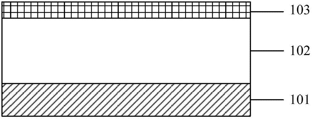
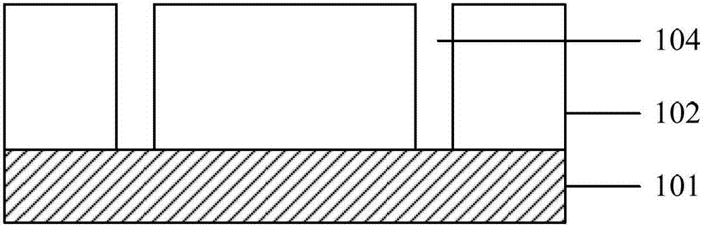
[0022] Step S1, depositing a dielectric layer on the substrate silicon wafer, coating a first photoresist on the dielectric layer, and forming a through-hole structure in the first photoresist, the first photoresist capable of forming a dura mater;

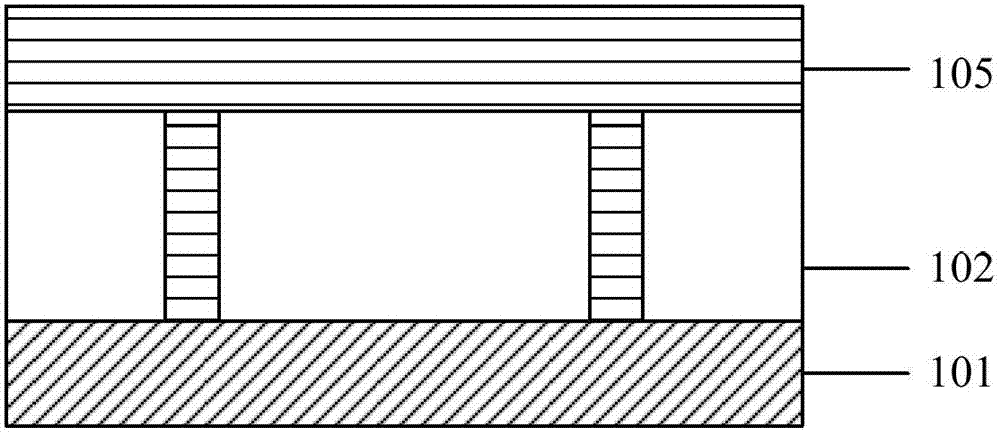
[0023] Step S2, in the same developing machine, coat the miniature cured material on the first photoresist pattern to cure the through-hole structure in the first photoresist, and heat the miniature cured material and reacting on the surface of the first photoresist, thereby forming an isolation film on the surface of the first photoresist;

[0024] Step S3, coating a second photoresi...


PUM


Abstract

The invention discloses a through hole priority copper interconnection manufacturing method, which comprises the following steps of: depositing a medium layer on a substrate, coating a first photoresist which can form a hard film on the medium layer, and forming a through hole structure in the first photoresist; coating a micro curing material on a first photoresist pattern for curing the through hole structure, heating for reacting the micro curing material with the surface of the first photoresist, and forming an isolating film on the surface of the first photoresist; coating a second photoresist on the cured first photoresist, and forming a channel structure positioned above the through hole structure in the second photoresist, wherein the isolating film is insoluble in the second photoresist; transferring the through hole structure and the channel structure into the medium layer; and continuing subsequent lead metal and through hole metal filling. In the method, the photoresist material which can form a hard film is used, so that an etching step is reduced, the manufacturing cost is lowered greatly, and the yield is increased effectively.

Description

technical field [0001] The present invention relates to a semiconductor manufacturing process, and in particular to a via-first copper interconnection manufacturing method. Background technique [0002] As the integration level of semiconductor chips continues to increase, the feature size of transistors continues to shrink. After entering the 130nm technology node, due to the limitation of aluminum's high resistance characteristics, copper interconnection technology gradually replaces aluminum interconnection and becomes the mainstream of metal interconnection. Due to the high hardness of copper, the dry etching process is not easy to implement, and the production of copper wires cannot be achieved by etching the metal layer like the production of aluminum wires. The widely used manufacturing method of copper wire is damascene technology called damascene process. [0003] Copper interconnects for damascene damascene structures can be achieved through a variety of process ...

Claims


Application Information

Patent Timeline
IPC IPC(8): H01L21/768
Inventor 毛智彪
Owner SHANGHAI HUALI MICROELECTRONICS CORP
Why Eureka
Try Eureka