

Novel grid structure for RF-LDMOS (Radio Frequency-Laterally Diffused Metal Oxide Semiconductor) device
A technology of RF-LDMOS and gate structure, applied in the direction of semiconductor devices, electrical components, circuits, etc., can solve the problem of reducing power gain and achieve the effect of reducing gate resistance and improving power gain
- Summary
- Abstract
- Description
- Claims
- Application Information
AI Technical Summary
Problems solved by technology
Method used
Image

Examples
Embodiment 1
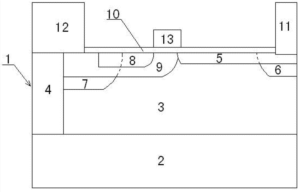
[0027] This embodiment describes an N-type LDMOS used in RF-LDMOS devices, its structure is as follows figure 2 As shown, it includes the RF-LDMOS basic structure 1, and the RF-LDMOS basic structure 1 includes the lowermost heavily doped substrate 2 region, the epitaxial layer 3 on the heavily doped substrate 2 region, and the epitaxial layer 3 Above the gate 13, the epitaxial layer 3 is provided with a heavily doped source region 8 and a heavily doped drain region 6, and the heavily doped source region 8 and the heavily doped drain region 6 are respectively located on different sides of the gate 13. On the side, a channel region 9 and a drain drift region 5 are sequentially arranged between the heavily doped source region 8 and the heavily doped drain region 6 in the epitaxial layer 3, and the channel region 9 and the The heavily doped source region 8 is in contact with the drain drift region 5, and a heavily doped connection or a trench 4 filled with a conductor is arranged...
Embodiment 2
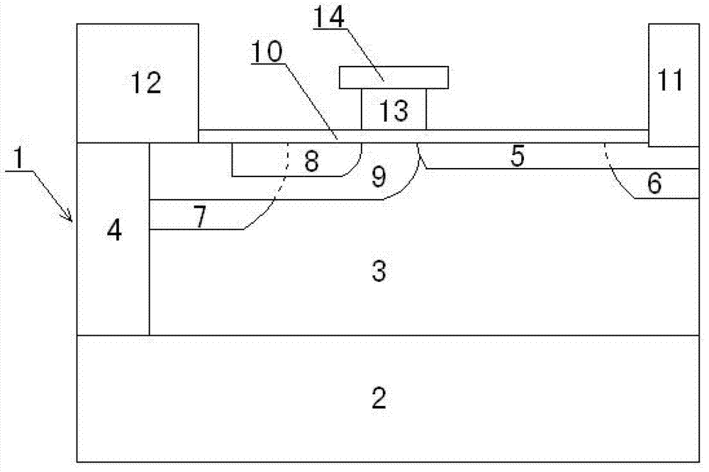
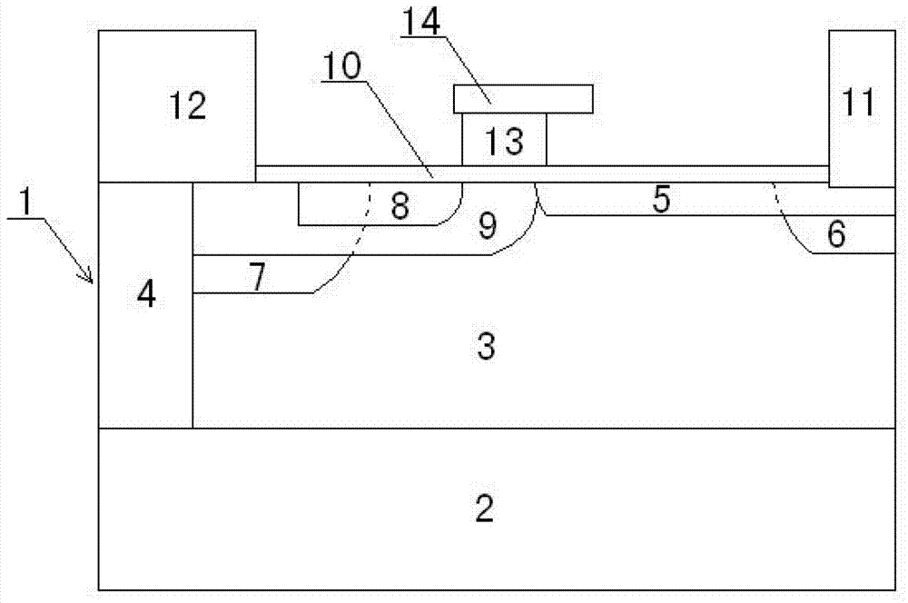
[0031] The basic structure of this embodiment is the same as that of Embodiment 1, except that the gate extension layer 14 covering the gate 13 completely covers the gate 13, and extends to the heavily doped source region 8 for a short distance, and to the heavily doped source region 8. The distance over which the drain region 6 extends is relatively long. In this way, the width of the heavily doped source region 8 can be made relatively small, which can reduce the series resistance of the section of the heavily doped source region 8 .
Embodiment 3
[0033] The basic structure of this embodiment is the same as that of Embodiment 1, except that the gate extension layer 14 covering the gate 13 completely covers the gate 13, and the distance extending to the heavily doped source region 8 is zero, and the distance extending to the heavily doped source region 8 is zero. The extended distance of the miscellaneous drain region 6 is relatively long.
[0034] Extending more toward the drain end, the gate extension layer 14 will have a long overlapping area with the drain drift region 5 below, and this overlapping area is equivalent to a field plate. When the amplitude of the input signal is relatively high, the gate extension layer 14 has a relatively high forward voltage. At this time, a part of electrons will be attracted into the drain drift region 5, which will reduce the resistance of the drain drift region 5 and reduce the conductivity. on-resistance, thereby improving efficiency. And when the amplitude of the input signal i...
PUM
 Abstract
Description
Claims
Application Information