

Power MOSFET with reduced dgate resistance
- Summary
- Abstract
- Description
- Claims
- Application Information
AI Technical Summary
Benefits of technology
Problems solved by technology
Method used
Image

Examples
embodiment 1
(Embodiment 1)
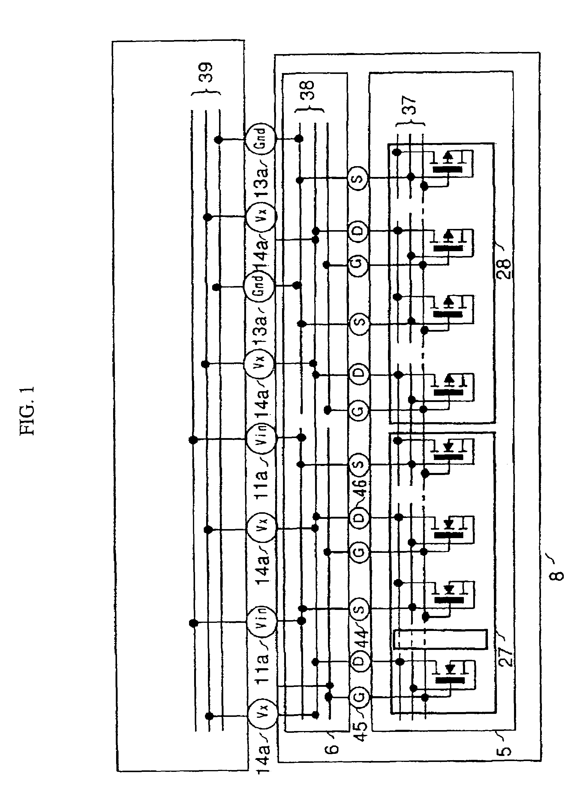
[0024]FIG. 1 shows a cross-sectional view illustration of a power semiconductor device in the present embodiment. In FIG. 1, numeral 5 designates a semiconductor chip, 6 a multilayer circuit board, 7 a printed circuit board, 8 a package, 37 wires formed on the semiconductor chip, 38 an electrode layer in the multilayer circuit board, and 39 an electrode layer in the printed circuit board. In FIG. 1, the power MOSFETs are shown in equivalent circuits. In the semiconductor chip 5, there are formed power MOSFET cells that occupy an area of 2 mm2 or more. N-channel power MOSFET 27 and a power MOSFET 28 are formed by a repetitive pattern of these power MOSFET cells.
[0025]In the present embodiment, the drain, gate and source of the power MOSFETs are connected to the electrode layer 38 of the multilayer circuit board 6 via drain bumps 46, gate bumps 45 and source bumps 44, respectively. It is difficult to reduce the gate resistance of the power MOSFETs that occupy large areas...
embodiment 2
(Embodiment 2)
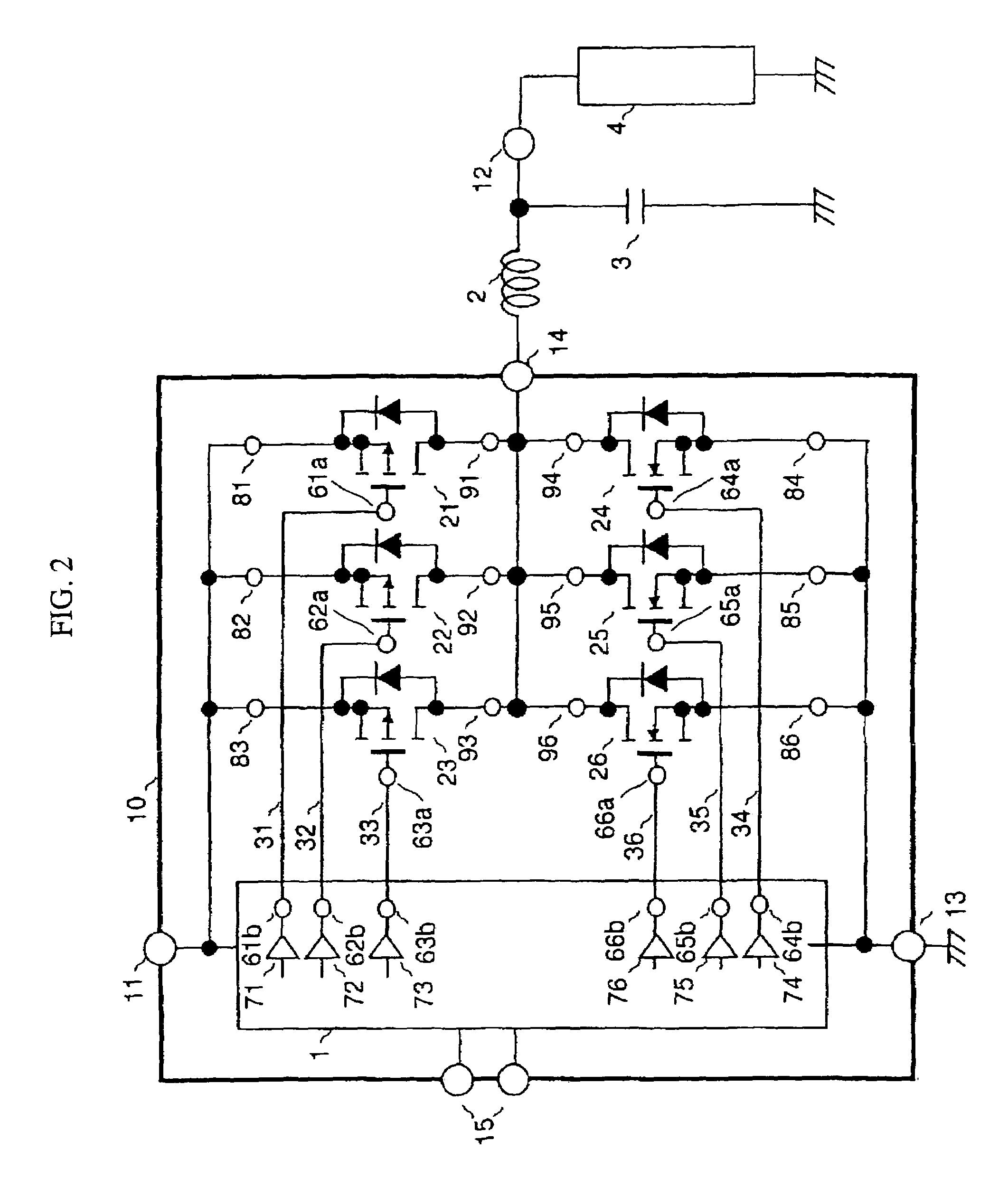
[0037]FIG. 7 shows a cross-sectional illustration view of the power semiconductor device according to Embodiment 2. This embodiment is based on a monolithic, vertical power MOSFET in which a drain electrode 9 on the back surface of the semiconductor chip 5 is connected to the printed circuit board 7 via drain bumps 46. Embodiment 2 differs from Embodiment 1 in that wiring to the electrode layer 39 on the printed circuit board 7 is achieved directly without using the multilayer circuit board 6. Further, in the present embodiment, the drain electrode 9 fabricated as part of the package 8 serves the function of the wire connecting to the drain bumps 46.
[0038]In the present embodiment, too, the gate wires are connected with low resistance via the gate bumps 45 formed on the two or more gate electrodes and the electrode layer 39 in the printed circuit board 7 outside the semiconductor chip 5. Thus, the resistance in the gate layer provided throughout the MOSFETs can be grea...
embodiment 3
(Embodiment 3)
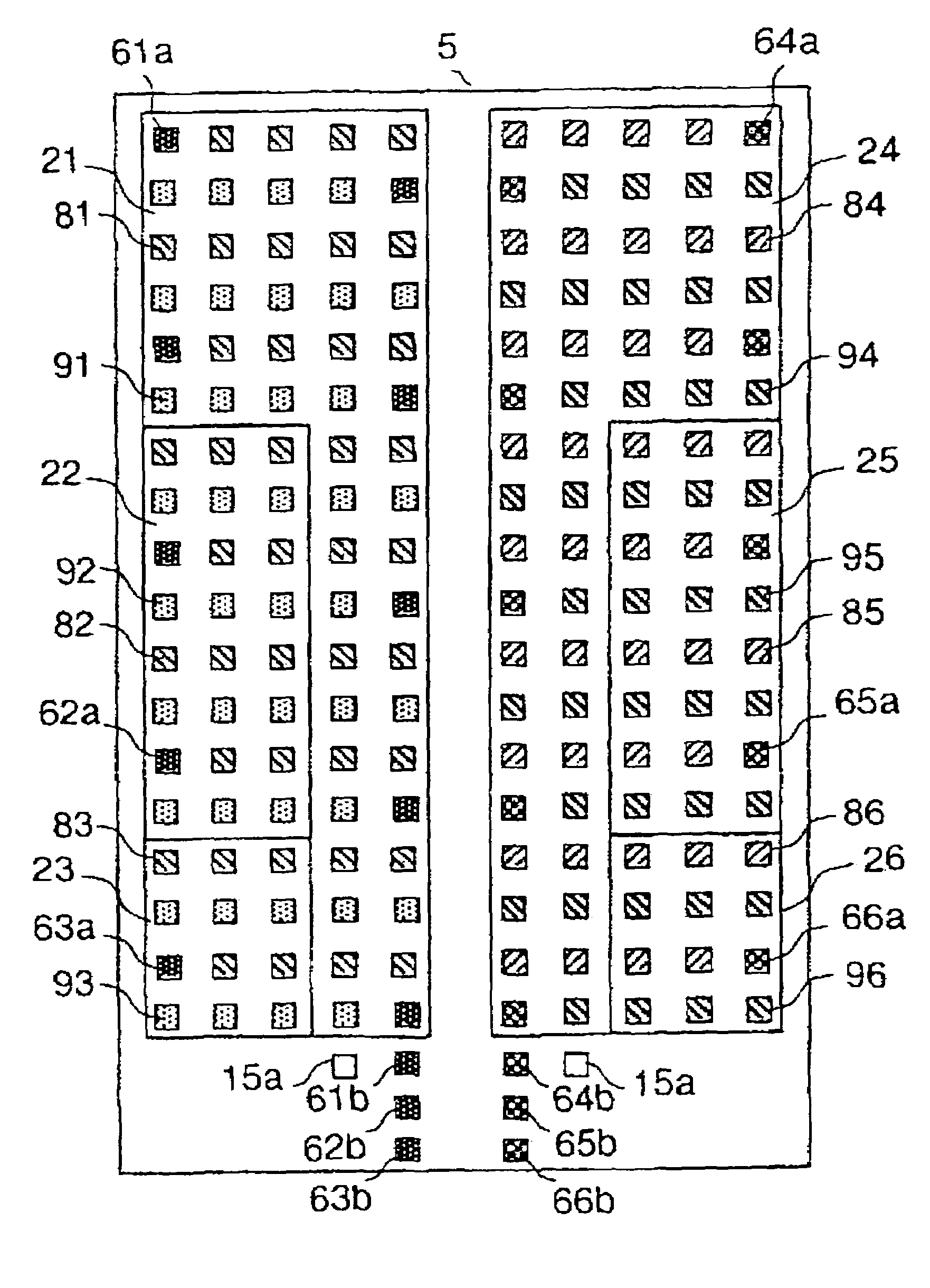
[0040]FIG. 10 shows a plan view of the power semiconductor device according to Embodiment 3. FIG. 11 shows a block circuit diagram of the power semiconductor device of Embodiment 3. In this embodiment, gate pads 42a and 42b, that are connected by the formation of the electrode layer 102a, are formed such that they are spaced apart from one another. The gate pad 42a is connected to the gate layer via wiring in the silicon chip of the power MOSFET 28, while the gate pad 42b is connected to the control circuit portion 100 for the power MOSFET 28.
[0041]In the present embodiment, while a gate pad 42 is provided for the external gate terminal, the gate pad 42 and the gate pad 42b may be commonly fabricated depending on the circuit design of the control circuit portion 100. In this embodiment, before completing connections for the gate pads 42a and 42b using the electrode layer 102a, a gate-to-source breakdown voltage can be measured on the power MOSFET 28 using the gate pad ...
PUM
 Abstract
Description
Claims
Application Information