Semiconductor light-emitting element

A light-emitting element and semiconductor technology, which is applied in the direction of semiconductor devices, electrical components, electric solid-state devices, etc., can solve problems such as difficulties, achieve good light extraction, improve light reflection, and reduce element resistance.

Active Publication Date: 2015-09-02
NICHIA CORP
View PDF16 Cites 0 Cited by
  • Summary
  • Abstract
  • Description
  • Claims
  • Application Information

AI Technical Summary

Problems solved by technology

Especially for the latter, in order to improve the power efficiency, it is necessary to reduce the element resistance such as Vf and improve the luminous characteristics and light extraction efficiency, so it is sometimes difficult.

Method used


Image

  • Semiconductor light-emitting element
  • Semiconductor light-emitting element
  • Semiconductor light-emitting element

Examples


Embodiment approach 1

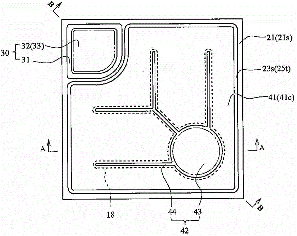
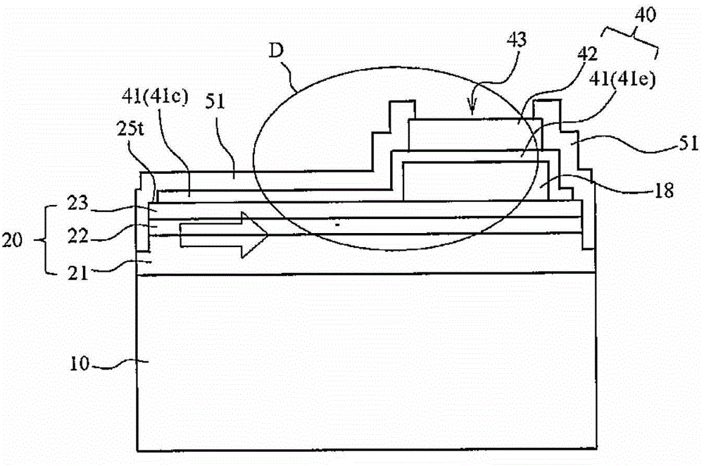
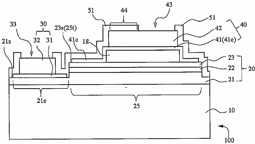
[0101] A specific example of LED100 of Embodiment 1 and its structure are demonstrated using FIG. 1. FIG. here, Figure 1A It is a schematic diagram illustrating a plane when viewing the LED according to Embodiment 1 from the electrode forming surface side, Figure 1B , Figure 1C is true Figure 1A A schematic diagram illustrating the cross-section on the A-A line and B-B line of Figure 1D , Figure 1E will be Figure 1C The schematic diagram after local enlargement, Figure 1E is description Figure 1D sketches of other forms.

[0102] The structure of the light-emitting element shown in FIG. 1 has a semiconductor structure 20 consisting of an n-type nitride semiconductor layer 21 in which a first conductivity type layer is laminated on a substrate 10 through a base layer (not shown) such as a buffer layer, The active layer 22 serving as the light emitting part and the p-type nitride semiconductor layer 23 of the second conductivity type layer are composed of a stacke...

Embodiment 1A

[0145] [Example 1A(1a)]2 2 2 2 <[embodiment 1C (1c)],

[0146] λ / 2n in Example 1B(1b) 2 Near, more specifically, at λ / 2n 2 ±λ / 4n 2 (λ / 4n 2 Above, 3λ / 4n 2 In the range below), better light output can be obtained. On the other hand, according to the comparison of Example 1A (1a) and Example 1C (1c), it can be seen that the thicker the insulating film, the higher the Vf tends to be. Vf becomes higher due to the first layer of the insulating film.

[0147] Next, in the above-mentioned Example 1 (research example, the structure of FIG. 1 ), the following study example, and Example 2 ( Figure 4 structure), Example 5 of Embodiment 7 ( image 3 structure) and the structures shown in the comparative examples of these examples, the film thickness of the first layer of ITO was changed between 20nm and 170nm to produce light-emitting elements respectively, and the following Figure 13 output characteristics shown. Here, in order to offset the difference in output due to the diff...

Embodiment approach 2

[0150] As Embodiment 2, in Example 1 of Embodiment 1, the shape of the extension portion 44 of the second electrode (p-electrode) is set to Figure 4 In the shape shown, the number of extensions is changed from 4 (Example 1) to 9, and a light-transmitting insulating film corresponding to the shape of the extensions (second layer) and electrodes is provided. , a substantially square (320 μm×320 μm) light-emitting element was produced with the same structure and dimensions as in Example 1.

[0151] In this light-emitting element, compared with Example 2, the number and area of ​​electrode extensions are larger, so phenomena such as current diffusion are improved. decreased, and the output of the element tended to be slightly lower than in Example 2.

[0152]Concretely, for comparison, in the same manner as the study examples of Example 1 (Examples 1A to 1C, 1a to 1c), under the condition that the second layer of the second electrode and the light-transmitting insulating film ar...


PUM


Abstract

The present invention provides a light emitting element capable or realizing at least one of, preferably, most of lower resistance, higher output, higher power efficiency (1m / W), higher mass productivity and lower cost of the element using a light transmissive electrode for an electrode arranged exterior to the light emitting structure. A semiconductor light emitting element including a light emitting section, a first electrode, and a second electrode on a semiconductor structure including first and second conductive type semiconductor layers, the first and the second electrodes being arranged on the first conductive type semiconductor layer and a second conductive type semiconductor layer of the light emitting section, respectively; and a light transmissive insulating film formed on at least one part of the second conductive type semiconductor layer; wherein the second electrode includes a first layer of a light transmissive conductive film for covering at least one part of the second conductive type semiconductor layer and a second layer which is arranged on at least one part of the light transmissive insulating film and which conducts to the first layer; a light reflecting part is formed on a surface side of the first layer, and a boundary region of the light transmissive insulating film and the semiconductor structure; and the second layer side surface of the light transmissive insulating film is distant from the semiconductor structure than the surface of the first layer is provided.

Description

[0001] This application is a divisional application of a patent application whose filing date is January 30, 2008, application number is 200810000273.0, and the invention name is "semiconductor light-emitting element". technical field [0002] The present invention relates to a semiconductor light-emitting element, in particular to an electrode structure of a light-emitting element. Background technique [0003] For light-emitting devices using nitride semiconductors, various studies have been conducted in order to obtain light emission in the near-ultraviolet to red region due to its wide bandgap characteristics. The general basic structure of a nitride semiconductor light-emitting element is a structure in which an n-type nitride semiconductor, an active layer, and a p-type nitride semiconductor are stacked on a substrate, and each layer is provided on a p-type layer and a partially exposed n-type layer. The structure of the electrode, the structure of the light-emitting e...

Claims


Application Information

Patent Timeline
Patent Type & Authority Patents(China)
IPC IPC(8): H01L33/42H01L33/02H01L33/38H01L33/44
CPCH01L33/405H01L2224/48247H01L33/38H01L33/46H01L2224/48091H01L33/02H01L2224/73265H01L2224/49107H01L33/42H01L33/44H01L2224/48465H01L2924/00014H01L2924/00
Inventor 佐野雅彦坂本贵彦榎村恵滋家段胜好
Owner NICHIA CORP
Why Eureka
Try Eureka