
Testing chip and chip testing system thereof

A technology for testing chips and chips to be tested, which is applied in the direction of electronic circuit testing, etc., can solve the problems of increasing measurement cost and time-consuming measurement process, and achieve the effect of reducing mass production cost and improving measurement accuracy

Inactive Publication Date: 2012-11-21
NOVATEK MICROELECTRONICS CORP
View PDF9 Cites 13 Cited by
  • Summary
  • Abstract
  • Description
  • Claims
  • Application Information

AI Technical Summary

Problems solved by technology

However, if a high-speed mass production machine is used to measure these characteristics of the chip, the measurement process will be very time-consuming and will increase a lot of measurement costs

Method used


Image

  • Testing chip and chip testing system thereof
  • Testing chip and chip testing system thereof
  • Testing chip and chip testing system thereof

Examples


Embodiment Construction

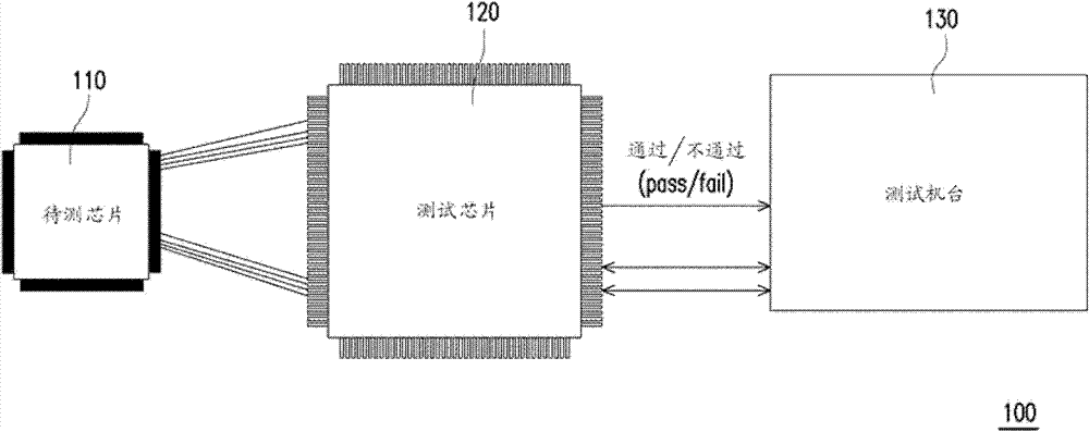
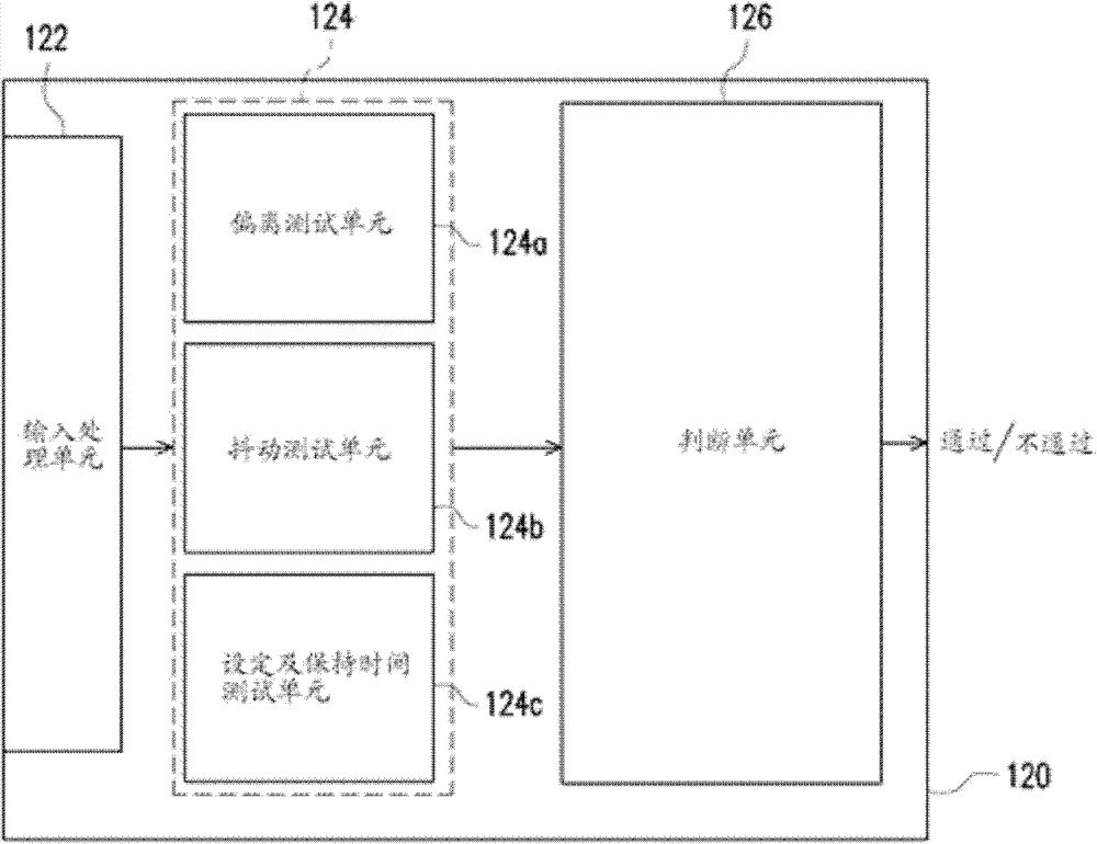
[0072] figure 1 It is a schematic diagram of the implementation of a chip testing system according to an embodiment of the present invention. Please refer to figure 1 The chip testing system 100 of this embodiment includes a chip to be tested 110, a testing chip 120, and a testing machine 130. Here, the test machine 130 utilizes test input data such as test vectors or test patterns to perform various electrical measurements on the chip 110 under test. Among them, at least for skew test, jitter test, and setup / hold time test, the chip test system 100 can use the test chip 120 to measure the chip under test 110. , In order to reduce the cost of mass production and improve the accuracy of measurement.

[0073] Therefore, in this embodiment, the testing machine 130 provides test input data to the chip under test 110 to send the signal under test to the test chip 120, and at the same time, the test machine 130 sets the test chip 120. Then, after receiving the test input data, the ch...


PUM


Abstract

The invention relates to a testing chip and a chip testing system thereof. The chip testing system comprises a chip to be tested, the testing chip and a testing machine; the chip to be tested is used for receiving the test input data and providing the test output data accordingly; the testing chip is used for carrying out at least one of the deviating test, the shaking test and the setting and maintaining time test to the chip to be tested according to the test input data and judging whether a testing result is in a preset range or not; and the testing machine is used for providing the test input data and inputting the test input data into the chip to be tested through the testing chip.

Description

Technical field [0001] The invention relates to a test element and a test system thereof, in particular to a test chip and a chip test system thereof. Background technique [0002] In recent years, the display panel technology has reached a mature stage, but with consumer demand, the size of the display panel is getting larger and the resolution is getting higher. However, as the resolution and size of the display panel increase, the operating frequency inside the panel will increase. At present, most of the transmission interfaces of the timing controller and the source driver in the display panel are transmitted by a dedicated clock interface. [0003] As the size and resolution of the display panel increase, the speed of the transmission interface is getting faster and faster, and the transmission quality thereof is also increasing. The relationship between the high-speed serial data and the clock of the dedicated clock interface, such as channel to channel skew, clock jitter,...

Claims


Application Information

Patent Timeline
Patent Type & Authority Applications(China)
IPC IPC(8): G01R31/28
Inventor 罗仁鸿
Owner NOVATEK MICROELECTRONICS CORP
Learn More