Automatic laser marking device for wafer resistor

A technology of automatic scribing and chip resistance, applied in laser welding equipment, welding equipment, metal processing equipment, etc., can solve the problems of general products without structure, difficulty in ultrasonic washing, unstable product quality, etc., to achieve compact structure and buffering effect. Good, well-structured effect

Active Publication Date: 2012-11-28
昆山市和博电子科技有限公司
View PDF7 Cites 9 Cited by
  • Summary
  • Abstract
  • Description
  • Claims
  • Application Information

AI Technical Summary

Problems solved by technology

[0003] With the quantification of the electronics industry and the continuous increase in production costs, a new chip resistor manufacturing process has emerged in the chip resistor industry in recent years, which is called "sputtering thin film process" in the industry, hereinafter referred to as thin film process. The biggest advantage is that the cost is greatly reduced compared with the thick film process, and it is more environmentally friendly than the thick film process. The electrodes and conductors in this process are sputtered. Sputtering can only cover the entire substrate, while The gap between each row of resistors is screen-printed water-soluble slurry before sputtering, which is called pickled film layer in the industry. After the sputtering is completed, the pickled film layer is washed off by ultrasonic water, thus effectively controlling The spacing between each row of resistors; however, although the pickled film layer is a water-soluble slurry, which in principle dissolves when it meets water, a layer of metal-like resistor conductor is also attached to the surface during sputtering, so On the one hand, it brings considerable difficulty to ultrasonic washing, because after the surface is attached with a resistance conductor, the water cannot penetrate into the water-soluble slurry layer, and the cleaning is often not clean, which brings instability to the product quality;
[0004] This shows that above-mentioned existing wafer resistor manufacturing process equipment obviously still has inconvenience and defect in structure and use, and urgently needs to be further improved
In order to solve the problems existing in chip resistance manufacturing equipment, relevant manufacturers have tried their best to find a solution, but no suitable design has been developed for a long time, and general products do not have a suitable structure to solve the above problems. Obviously, it is a problem that relevant industry players are eager to solve.

Method used


Image

  • Automatic laser marking device for wafer resistor
  • Automatic laser marking device for wafer resistor
  • Automatic laser marking device for wafer resistor

Examples


Embodiment Construction

[0033] In order to further explain the technical means and effects of the present invention to achieve the intended purpose of the invention, the specific implementation, structure and characteristics of the chip resistance laser automatic scribing equipment proposed according to the present invention will be described below in conjunction with the accompanying drawings and preferred embodiments. And its effect, detailed description is as follows.

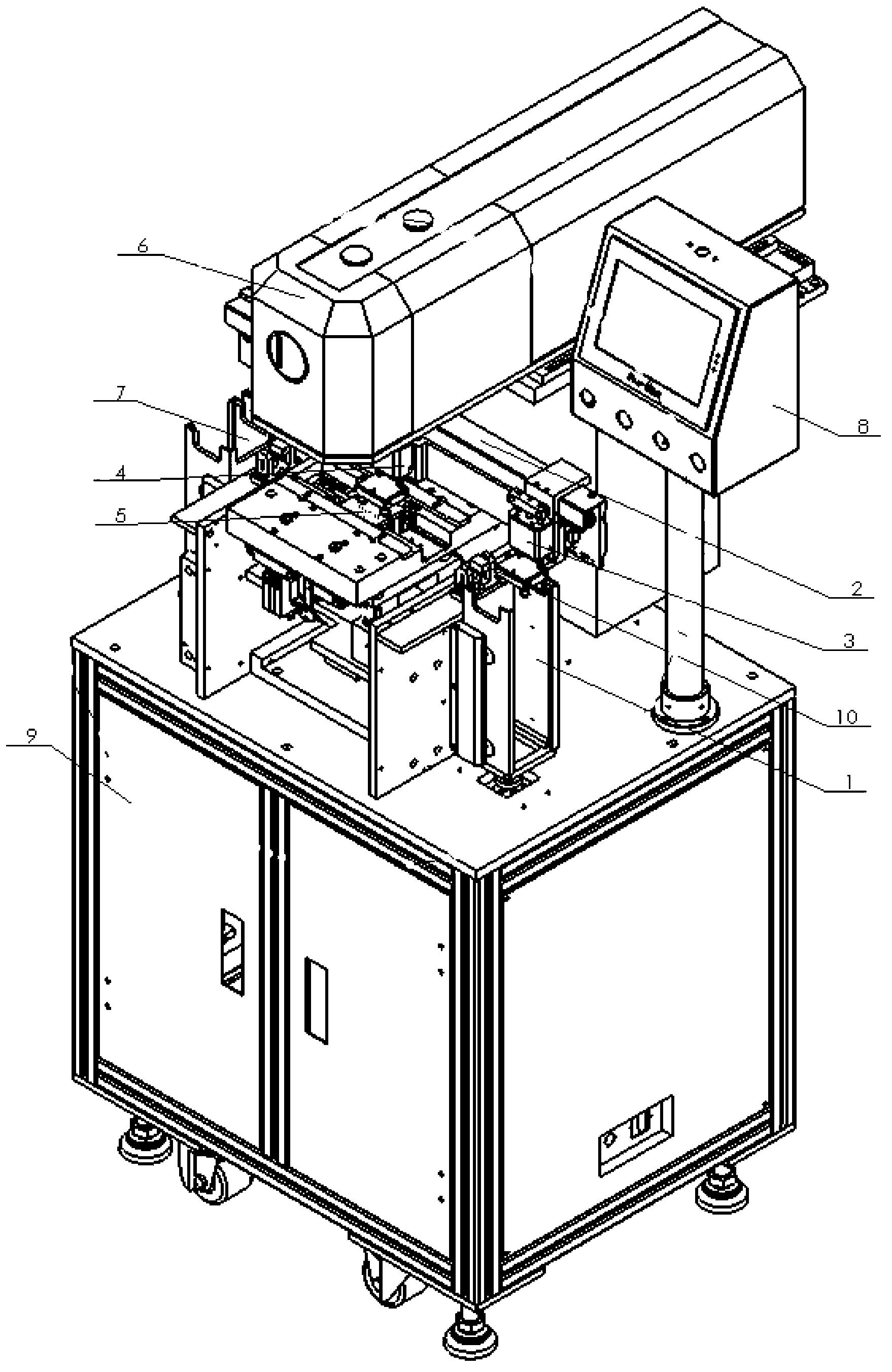
[0034] see figure 1A chip resistance laser automatic scribing equipment, including a frame 9, a receiving mechanism, used to support the substrate to be processed or transport the processed substrate to the receiving bin; there are two receiving mechanisms, one for A second vacuum suction cup suction mechanism 3 for holding the substrate to be processed, a first vacuum suction cup suction mechanism 4 for transporting the processed substrate to the receiving bin, and the first vacuum suction cup is movably connected to the conveying...


PUM

PropertyMeasurementUnit
sizeaaaaaaaaaa
thicknessaaaaaaaaaa

Abstract

The invention discloses an automatic laser marking device for a wafer resistor, which comprises a frame, a receiving mechanism, a conveying mechanism, an air blowing mechanism, a six-wheel eccentric link center positioning mechanism, an optical fiber laser device and a control box, wherein the receiving mechanism is used for holding a to-be-processed base plate or conveying the processed base plate to a receiving bin; the receiving mechanism is moveably connected with the conveying mechanism; the receiving mechanism can move on the conveying mechanism; a conveying bin is arranged on the lower part at one end of the conveying mechanism; the receiving bin is arranged on the lower part at the other end of the conveying mechanism; the six-wheel eccentric link center positioning mechanism is arranged at the lower end on the middle part of the conveying mechanism; the air blowing mechanism is used for performing air-blowing dust-removing treatment on the to-be-processed base plate held by the receiving mechanism; the six-wheel eccentric link center positioning mechanism is used for positioning the to-be-processed base plate held by the receiving mechanism; the optical fiber laser device is used for cutting lines for the base plate positioned by the six-wheel eccentric link center positioning mechanism; and the control box is used for controlling the receiving mechanism, the conveying mechanism, the air blowing mechanism, the six-wheel eccentric link center positioning mechanism and the optical fiber laser device to work.

Description

technical field [0001] The invention relates to an electronic passive component device, in particular to a chip resistance laser automatic scribing device. Background technique [0002] In the past, the "conductors" and "electrodes" of chip resistors were mostly screen-printed. The main body of chip resistors was a ceramic sheet, which was generally divided into a medium substrate and a small substrate. The sizes were 60*70mm, 50*60mm, and the thickness was 0.5 About mm, each substrate varies from hundreds of resistors to thousands of resistors depending on the type and specification of the resistors. There is a certain gap between each row of resistors. The distance between each resistor in the screen printing process is It is realized through a special customized "screen", which is collectively referred to as "printing thick film film process" in the industry, hereinafter referred to as thick film process. [0003] With the quantification of the electronics industry and t...

Claims


Application Information

Patent Timeline
Patent Type & Authority Applications(China)
IPC IPC(8): B23K26/38B23K26/14B23K26/42B23K26/142B23K26/70
Inventor 李永传徐明哲李刚陈海滨黄斌马新升
Owner 昆山市和博电子科技有限公司
Why Eureka
Try Eureka