Electroluminescence panel and manufacturing process therefor

A technology of electroluminescence and manufacturing method, which is applied in electroluminescence light source, semiconductor/solid-state device manufacturing, light source and other directions, and can solve problems such as saddle deformation of glass cover sheet

Inactive Publication Date: 2005-02-02
SANYO ELECTRIC CO LTD
View PDF2 Cites 6 Cited by
  • Summary
  • Abstract
  • Description
  • Claims
  • Application Information

AI Technical Summary

Problems solved by technology

However, with these methods, the position of the cover glass is shifted during the bonding process, and the cover glass may be deformed in a saddle shape.

Method used


Image

  • Electroluminescence panel and manufacturing process therefor
  • Electroluminescence panel and manufacturing process therefor
  • Electroluminescence panel and manufacturing process therefor

Examples


Embodiment 1

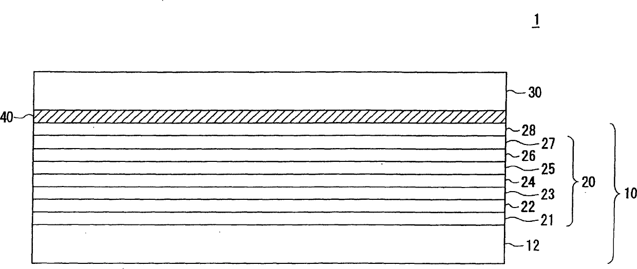
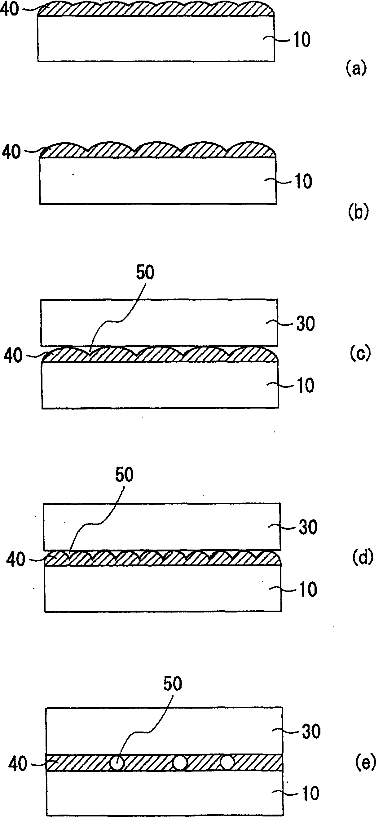
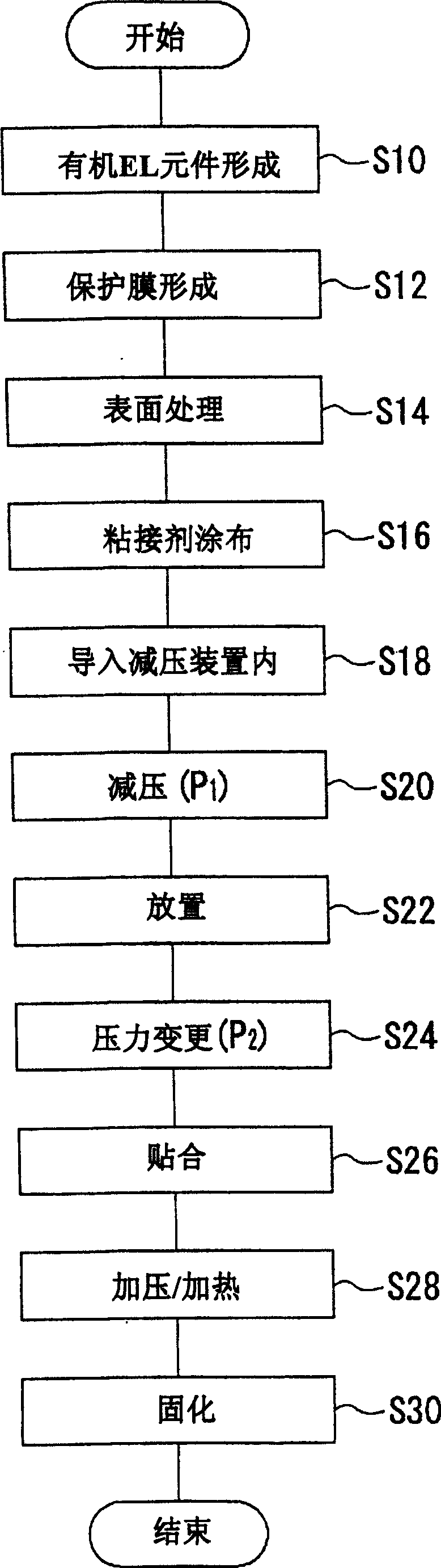
[0050]On the organic EL element 20 formed into a film on the glass substrate 12 , a protective film 28 made of an inorganic layer of SiN is laminated to manufacture the element substrate 10 . The element substrate 10 is 2.2 inches in length x 2.2 inches in width; the number of pixels is 220 pixels in length x 176 pixels in width. In the horizontal direction, a total of three types of pixels R, G, and B are arranged on one pixel. The size of the pixel is 0.198 mm in the vertical direction as the long side, and 0.066 mm in the horizontal direction as the short side in each of the R, G, and B pixels. The surface of the element substrate 10 is subjected to plasma treatment with argon. At this time, the contact angle is 10° or less. An ultraviolet UV-curable epoxy resin with a viscosity of 2 Pascal seconds is coated on the surface of the element substrate 10 by screen printing to improve uniformity. The element substrate 10 coated with the adhesive 40 is placed in the chamber of...

Embodiment 2

[0052] In Example 2, surface treatment was performed on both the element substrate 10 and the sealing substrate 30 . In addition, the organic EL panel 1 was manufactured in the same procedure as in Example 1. The number of tiny spaces in the organic EL panel 1 manufactured in this embodiment is 6 per diagonal inch with a diameter of 0.2 mm or less.

Embodiment 3

[0054] In Example 3, in the procedure shown in Example 1, the surface treatment of the substrate was not performed, and in the bonding process, as shown by the solid line in FIG. substrate. The number of minute spaces of the organic EL panel 1 manufactured in this embodiment is 5 per 1 inch of the diagonal for those with a diameter of 0.2 mm or less.


PUM

PropertyMeasurementUnit
viscosityaaaaaaaaaa
viscosityaaaaaaaaaa

Abstract

A method for manufacturing an electroluminescence panel comprises a step of forming an organic electroluminescence element (S10) on a glass substrate; a step of forming a protective film (S12) on the organic electroluminescence element; a step of performing an ozone treatment or plasma treatment (S14) on a surface of the glass substrate or a sealing substrate; a step of depositing an adhesive (S16) on the surface of the glass substrate or the sealing substrate, through a screen printing process; a step of disposing the glass substrate and the sealing substrate in a chamber (S18) of a pressure reduction device; a step of reducing pressure to P1 (S20) in the chamber; a step of leaving the substrate until foaming of volatile components contained in the adhesive is stabilized (S22); a step of suppressing foaming (S24) of the volatile components by increasing the pressure to P2 in the chamber; a step of bonding the substrates (S26); a steps of applying pressure and heat (S28) to the bonded substrates so as to remove micro spaces; and a step of hardening (S30) the adhesive.

Description

technical field [0001] The present invention relates to an electroluminescent panel, and more particularly to an electroluminescent panel having a structure in which a sealing substrate is attached to a substrate on which electroluminescent elements are formed, and a method for manufacturing the same. Background technique [0002] In recent years, with the diversification of information equipment, there has been an increasing demand for flat panel display elements that consume less power than conventional cathode ray tubes (CRTs). As one of such flat-panel display elements, an organic electroluminescent (hereinafter referred to as "organic EL") element having characteristics such as high efficiency, thinness, light weight, and small dependence on viewing angles has attracted attention. The development of displays with EL elements is progressing. [0003] Among the organic EL elements, organic EL elements using organic materials as the light-emitting layer can change the col...

Claims


Application Information

Patent Timeline
Patent Type & Authority Applications(China)
IPC IPC(8): H05B33/10H01J1/62H01L51/50H01L51/52H05B33/04H05B33/14
CPCH01L51/5246H10K50/8426H05B33/10
Inventor 白玖久雄原田学
Owner SANYO ELECTRIC CO LTD
Why Eureka
Try Eureka