Avalanche photodiode and avalanche photodiode array
An avalanche photoelectric and diode technology, applied in circuits, electrical components, electrical solid devices, etc., can solve the problem of no multiplication function and achieve the effect of large aperture ratio
- Summary
- Abstract
- Description
- Claims
- Application Information
AI Technical Summary
Problems solved by technology
Method used
Image
Examples
Embodiment approach 1
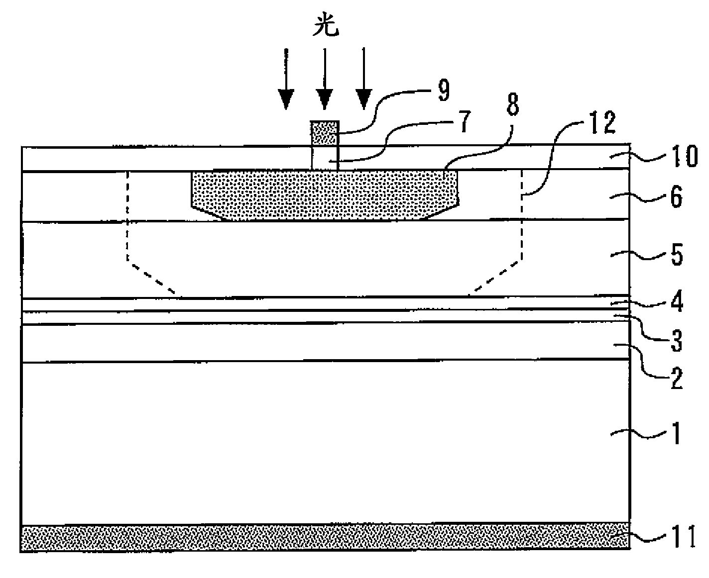
[0039] figure 1 It is a plan view showing the avalanche photodiode according to Embodiment 1 of the present invention. figure 2 is along figure 1 Sectional view of I-II. On the main surface of the n-type InP substrate 1, an n-type InP layer buffer layer 2, an avalanche multiplication layer 3 composed of doped AlInAs with a thickness of 0.15-0.4 μm, and a p-type InP electric field buffer layer with a thickness of 0.03-0.06 μm are sequentially stacked. layer 4, a light absorbing layer 5 made of doped InGaAs with a thickness of 2-3 μm, a doped InP window layer 6 with a thickness of about 2 μm, and an InGaAs contact layer 7. A p-type impurity region 8 is provided in a part of the InP-doped window layer 6 .
[0040] The impurity concentration of the n-type InP substrate is about 5×10 18 cm -3 , the impurity concentration of the p-type InP electric field buffer layer 4 is 0.5~1×10 18 cm -3 , the impurity concentration of the p-type impurity region 8 is 1×10 19 ~1×10 20 cm ...
Embodiment approach 2
[0056] Figure 7 It is a plan view showing an avalanche photodiode according to Embodiment 2 of the present invention. The linear p-side electrode 9 has a plurality of linear electrode portions 9 a , 9 b , and 9 c arranged parallel to each other, and an electrode portion 9 d orthogonal to and commonly connected to the plurality of electrode portions 9 a , 9 b , and 9 c .
[0057] The interval a is 20 μm. The interval e between adjacent electrode portions 9a, 9b, and 9c is 40 μm. The width w of the electrode portions 9a, 9b, and 9c is 5 μm, respectively. The p-type impurity region 8 is rectangular or rounded in plan view. The length b of the p-type impurity region 8 is longer than the width f.
[0058] Next, effects of Embodiment 2 will be described. In Embodiment 1, since one linear p-side electrode 9 is used, the width c of the p-type impurity region 8 is limited (since the interval a is 30 μm or less, the maximum value of the width c=2×30 μm+electrode width w) . On th...
Embodiment approach 3
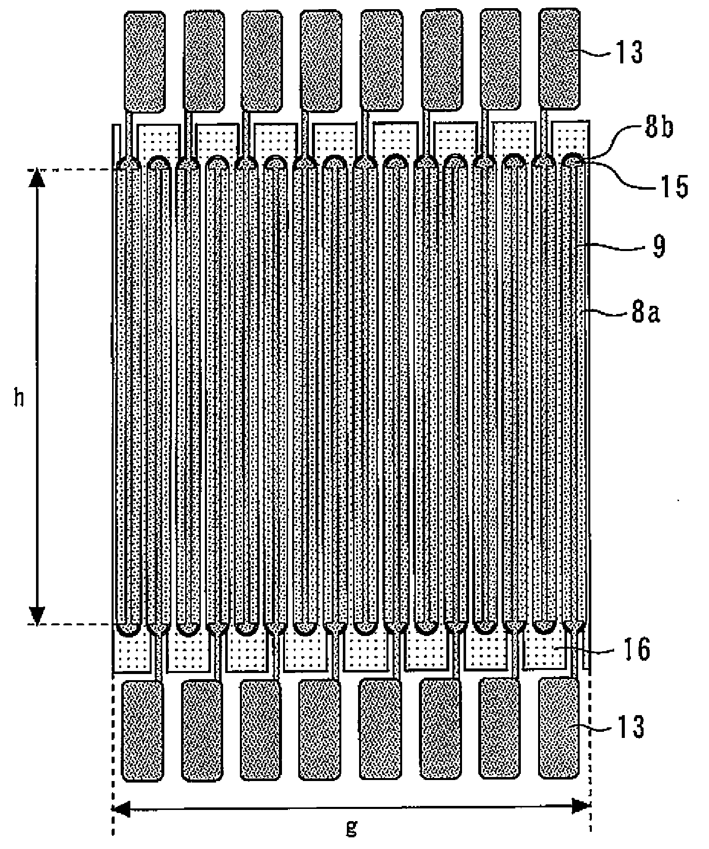
[0062] Figure 8 It is a top view showing an avalanche photodiode according to Embodiment 3 of the present invention. The p-type impurity region 8 has a rectangular region 8a in plan view and two semicircular regions 8b joined to the two short sides of the rectangular region 8a, respectively. By joining the semicircular region 8b to the rectangular region 8a in this way to eliminate the corners, electric field concentration at the corners of the p-type impurity region 8 can be avoided.
PUM
 Abstract
Description
Claims
Application Information


