Semiconductor apparatus and method of fabrication for a semiconductor apparatus

A manufacturing method and semiconductor technology, applied in the direction of semiconductor devices, final product manufacturing, sustainable manufacturing/processing, etc., to achieve the effects of improving stability, improving passivation quality, and high flexibility

Active Publication Date: 2012-11-28
韩华思路信
View PDF4 Cites 10 Cited by
  • Summary
  • Abstract
  • Description
  • Claims
  • Application Information

AI Technical Summary

Problems solved by technology

This additional requirement on the passivation layer often leads to a compromise of suboptimal surface passivation

Method used


Image

  • Semiconductor apparatus and method of fabrication for a semiconductor apparatus
  • Semiconductor apparatus and method of fabrication for a semiconductor apparatus
  • Semiconductor apparatus and method of fabrication for a semiconductor apparatus

Examples


Embodiment Construction

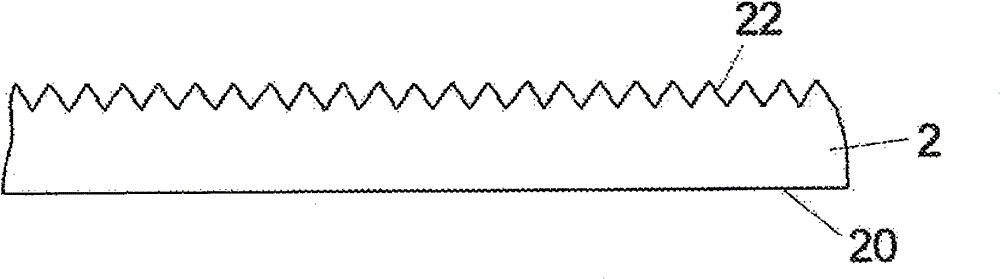
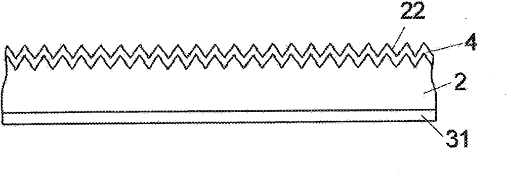
[0045] The manufacture of a solar cell 1 with surface passivation on both sides according to a possible embodiment is described below with reference to FIGS. 1a-1e. As noted in the background section of this specification, these considerations apply equally to other semiconductor devices than solar cells. 1 a shows a cross-section of a semiconductor layer 2 , wherein the semiconductor layer 2 comprises a semiconductor layer surface 20 forming a solar cell rear 20 facing backlight and a further semiconductor layer surface 22 forming a solar cell front 22 facing light. The surface 20 of the semiconductor layer is preferably textured (shown as a zigzag pattern in the figure) to improve efficiency.

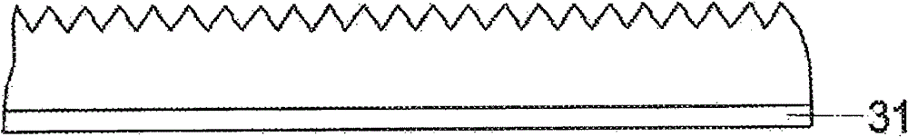
[0046] According to FIG. 1 b, a passivation sublayer 31 is applied to the semiconductor layer surface 20 for chemical passivation, wherein this sublayer can also serve as a diffusion barrier in a subsequent doping step of the further semiconductor layer surface 22 layer. After this ...


PUM


Abstract

The invention relates to a semiconductor apparatus (1) and a method of fabrication for a semiconductor apparatus (1), wherein the semiconductor apparatus (1) comprises a semiconductor layer (2) and a passivation layer (3), arranged on a surface of the semiconductor layer (2), for passivating the semiconductor layer surface (20), wherein the passivation layer (3) comprises a chemically passivating passivation layer element (31) and a field-effect-passivating passivation layer (33) which are arranged above one another on the semiconductor layer surface (20). The semiconductor apparatus is preferably a solar cell.

Description

technical field [0001] The present invention relates to a semiconductor device and a method of manufacturing the semiconductor device. Background technique [0002] One of the constraints on solar cell efficiency is the recombination of charge carriers at the semiconductor surface of the solar cell with surface states that promote recombination activity. These recombined charge carriers are then no longer available for current generation. To reduce recombination, the solar cell surface must be passivated by reducing the recombination activity of charge carriers via surface states. [0003] For surface passivation, there are in principle two different method. As a result, for surface passivation, firstly the number of surface states can be reduced. This so-called chemical passivation is achieved by chemical saturation of free surface bonds (so-called dangling bonds), for example in the case of semiconductor solar cells by silicon oxide layers (SiO 2 layer) by thermal gro...

Claims


Application Information

Patent Timeline
Patent Type & Authority Applications(China)
IPC IPC(8): H01L31/18H01L31/0216
CPCH01L31/02167Y02E10/50H01L31/1868Y02E10/547Y02P70/50
Inventor 皮特·恩格哈罗伯特·塞甘威廉颂·马蒂杰斯·马林·凯塞尔斯基杰斯·丁厄曼斯
Owner 韩华思路信
Why Eureka
Try Eureka