Method for forming metal pattern on surface of insulator

A metal pattern and insulator technology, applied in the field of forming metal patterns on the surface of insulators, can solve problems such as increasing the production cost, and achieve the effects of low cost and simple process

Inactive Publication Date: 2012-12-05
SHANGHAI AMPHENOL AIRWAVE COMM ELECTRONICS CO LTD
View PDF6 Cites 9 Cited by
  • Summary
  • Abstract
  • Description
  • Claims
  • Application Information

AI Technical Summary

Problems solved by technology

The disadvantage of this solution is that it needs to use a special insu...

Method used


Image

  • Method for forming metal pattern on surface of insulator
  • Method for forming metal pattern on surface of insulator
  • Method for forming metal pattern on surface of insulator

Examples


Embodiment Construction

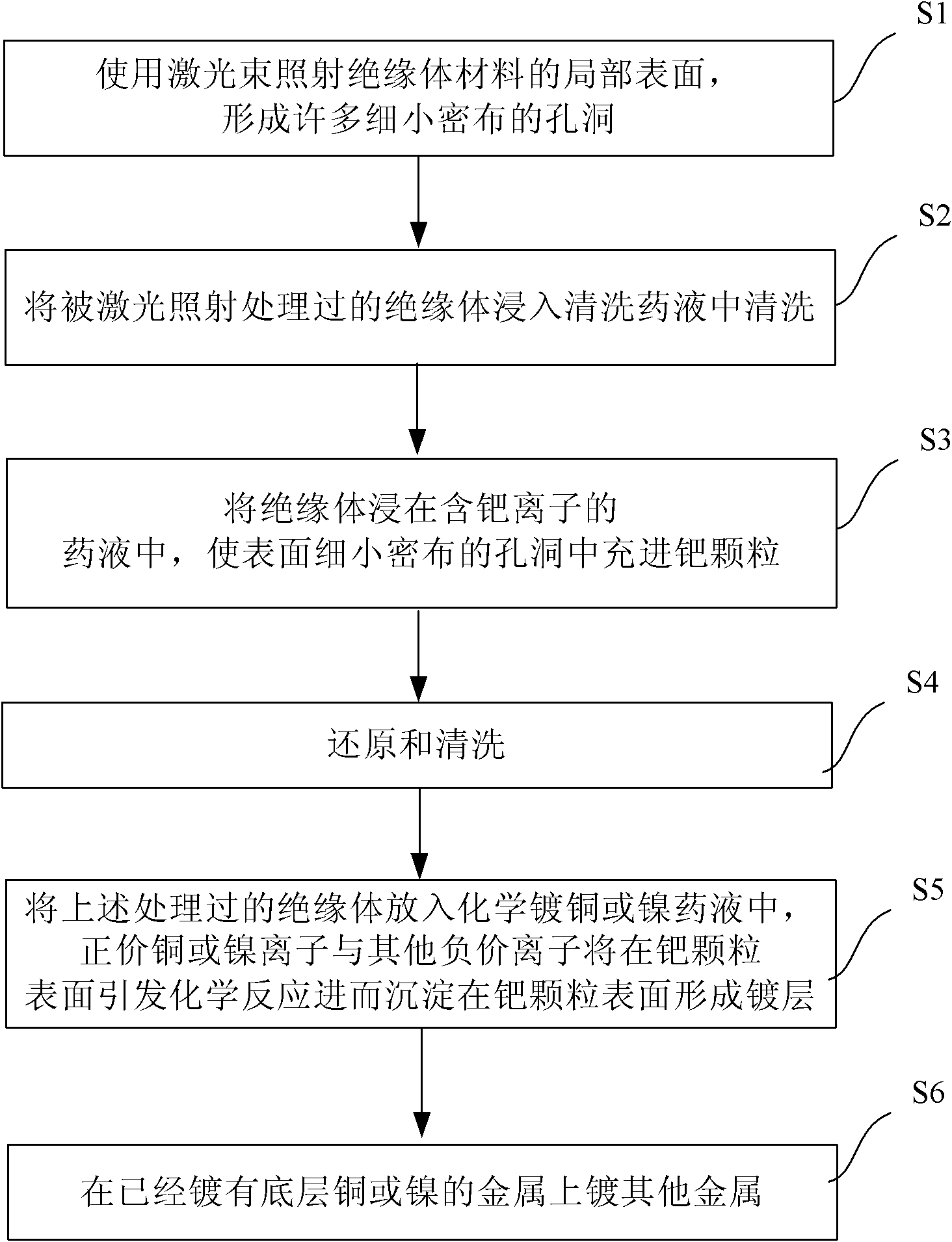
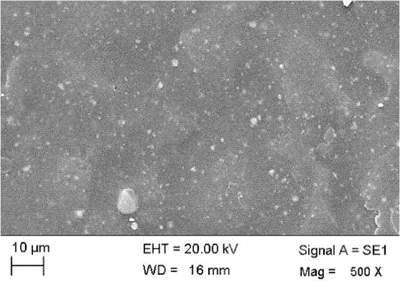
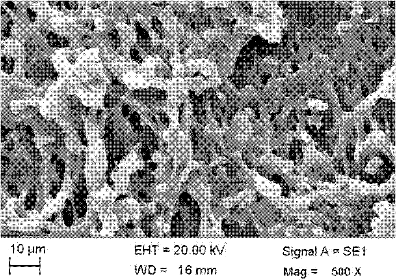
[0017] In summary, the present invention utilizes the property that a certain wavelength of laser light, such as infrared 1064nm laser light, can be absorbed by specific insulator materials, such as commonly used engineering plastics PC, PC / ABS, and PA, to generate heat. The laser beam is irradiated on the surface of the insulator, and the laser is focused on the surface of the insulator to form a very small spot. The laser hits the surface of the irradiated tiny area in the form of pulses. Form many fine and dense pores. Figure 2A and Figure 2B Shown is the surface morphology of the polycarbonate surface before and after laser irradiation. Such fine and dense pores can absorb metals such as palladium as an electroless plating medium, thus becoming a pavement for subsequent electroless plating.

[0018] Refer below figure 1 A flow of a method for forming a metal pattern on the surface of an insulator according to an embodiment of the present invention will be described. ...


PUM


Abstract

The invention relates to a method for forming a metal pattern on the surface of an insulator, which comprises the following steps of: using a laser beam to irradiate a local surface on an insulator material, on which the metal pattern is to be formed; soaking the insulator subjected to laser irradiation processing into cleaning liquid medicine to clean the insulator and removing attachments which are covered on the surface of holes and are formed due to gasification; soaking the insulator into liquid medicine containing palladium ions so as to fill ensure palladium particles into the holes which are fine and are densely distributed on the surface of the insulator; and placing the insulator into chemical copper or nickel plated liquid medicine, so that the chemical reaction is caused by positive valence copper or nickel ions and other negative valence ions on the surfaces of the palladium particles and the positive valence copper or nickel ions and the other negative valence ions are further precipitated on the surfaces of the palladium particles to form a coating. Compared with the prior art, the method disclosed by the invention has the advantages that only the local surface of a common insulator needs to be plated with the metal pattern instead of all the surface and the method does not depend on any special material containing particles, and thus, the method has simple process and lower cost.

Description

technical field [0001] The invention relates to a method for forming a metal pattern on the surface of an insulator. Background technique [0002] In the manufacture of structures such as antennas and circuits, it is often necessary to form metal patterns in local areas on the surface of insulator materials. At present, the methods for accurately making local metal patterns are listed as follows: [0003] 1. Soak the insulators in different chemical solutions to make the surface swell and then roughen it to form densely covered fine holes; then immerse the treated insulators in the ionic palladium solution to make the surface with metal palladium ; Then put the insulator into a chemical solution containing positive copper ions or nickel ions, and plate the entire surface with metal; finally, partially etch to remove the metal outside the pattern to form a metal pattern. The disadvantage of this solution is that the process of plating the entire surface of the insulator wit...

Claims


Application Information

Patent Timeline
IPC IPC(8): B41M3/00
Inventor 满方明
Owner SHANGHAI AMPHENOL AIRWAVE COMM ELECTRONICS CO LTD
Why Eureka
Try Eureka