Interposer and electronic device using the interposer
A technology for electronic devices and interposers, which is applied to semiconductor/solid-state device parts, circuits, electrical components, etc., and can solve the problems of low thermal expansion rate of inorganic insulating materials, damage to connection parts, and reduced electrical reliability of electronic devices.
- Summary
- Abstract
- Description
- Claims
- Application Information
AI Technical Summary
Problems solved by technology
Method used
Image

Examples
no. 1 approach
[0023] Hereinafter, an electronic device including the interposer according to the first embodiment of the present invention will be described in detail based on the drawings.
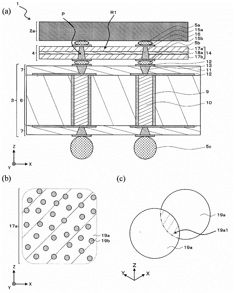
[0024] figure 1 The electronic device 1 shown in (a) is a device used in electronic equipment such as various audio-visual equipment, household electrical appliances, communication equipment, computer equipment or its peripheral equipment, and is electrically connected to external circuits such as female cards. The electronic device 1 includes: an electronic component 2; a wiring substrate 3 on which the electronic component 2 is mounted; an interposer 4 interposed between the electronic component 2 and the wiring substrate 3; The first bump 5a; the second bump 5b electrically connects the interposer 4 and the wiring board 3; and the third bump 5c electrically connects the wiring board 3 and an external circuit.
[0025] The electronic component 2 is mounted on the wiring board 3 via the interposer 4 ...
no. 2 approach
[0121] Next, based on Figure 5 , the electronic device including the interposer according to the second embodiment of the present invention will be described in detail. In addition, the description of the structure similar to the said 1st Embodiment is abbreviate|omitted.
[0122] The second embodiment is different from the first embodiment in that the interposer 4 is not interposed between the wiring board and the electronic component, but is interposed between the electronic components 2 that are separated from each other in the thickness direction. The interposers 4 are alternately stacked in the thickness direction to form the electronic device 1 . Therefore, three-dimensional mounting of the electronic component 2 can be realized, and the electronic device 1 can be miniaturized and signal transmission characteristics can be improved.
[0123] The electronic device 1 is electrically connected to an external circuit such as a female via the third bump 5c connected to the...
no. 3 approach
[0148] Next, based on Figure 7 , the electronic device including the interposer according to the third embodiment of the present invention will be described in detail. It should be noted that descriptions of the same configurations as those of the first and second embodiments described above are omitted.
[0149] The third embodiment is the same as the second embodiment, electronic components 2 and interposers 4 are alternately stacked in the thickness direction to form an electronic device 1, but the electrical connection method of the alternately stacked electronic components 2 and interposers 4 is the same as that of the second embodiment. different.
[0150] Hereinafter, the electrical connection form of the alternately stacked electronic components 2 and the interposer 4 will be specifically described.
[0151] Like the second embodiment, the first conductive layer 15a connected to the upper end of the through conductor 16 of the first interposer 4a is electrically con...
PUM
| Property | Measurement | Unit |
|---|---|---|
| thickness | aaaaa | aaaaa |
| particle diameter | aaaaa | aaaaa |
| particle diameter | aaaaa | aaaaa |
Abstract
Description
Claims
Application Information
 - R&D
- Intellectual Property
- Life Sciences
- Materials
- Tech Scout
- Unparalleled Data Quality
- Higher Quality Content
- 60% Fewer Hallucinations
Browse by: Latest US Patents, China's latest patents, Technical Efficacy Thesaurus, Application Domain, Technology Topic, Popular Technical Reports.
© 2025 PatSnap. All rights reserved.Legal|Privacy policy|Modern Slavery Act Transparency Statement|Sitemap|About US| Contact US: help@patsnap.com