Fast generating method of user-customizable PLD (programmable logic device) layouts

A programming logic and user-customized technology, applied in the direction of instruments, special data processing applications, electrical digital data processing, etc., can solve problems such as low layout efficiency, insufficient FPGA IP cores to meet resource requirements, and long time required to generate layouts, etc.

Inactive Publication Date: 2012-12-19
FUDAN UNIV
View PDF0 Cites 21 Cited by
  • Summary
  • Abstract
  • Description
  • Claims
  • Application Information

AI Technical Summary

Problems solved by technology

[0004]Different SoC designs often have different requirements for logic resources, which results in a waste of resources if the FPGA IP core is too large, and if the FPGA IP is too small Not enough cores to meet resource requirements
Therefore, a kind of FPGA layout generation tool that can be required according to user scale is very necessary, before the tool of the present invention proposes,

Method used


Image

  • Fast generating method of user-customizable PLD (programmable logic device) layouts
  • Fast generating method of user-customizable PLD (programmable logic device) layouts
  • Fast generating method of user-customizable PLD (programmable logic device) layouts

Examples


Embodiment Construction

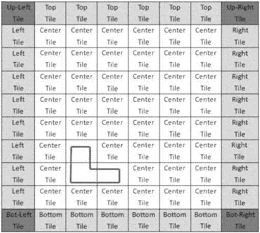
[0083] Since the layout of commercial FPGA chips is not public, we cannot obtain its layout files. Therefore, the present invention selects the cell layout of the FDP3P7 series FPGA chips developed by Fudan University ASIC and State Key Laboratory of Systems as an example, and illustrates how to utilize the method proposed by the present invention to generate a 16 x 20 array-scale FPGA that is set by a user territory.

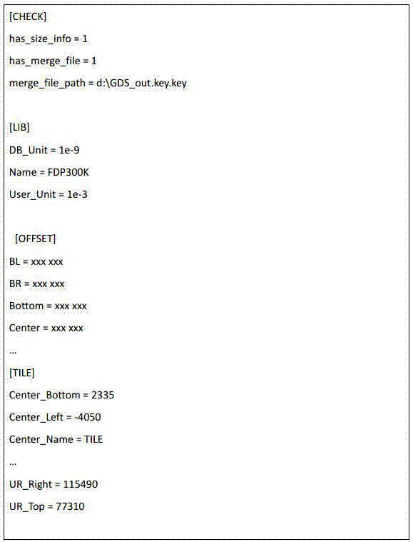
[0084] First, create a chip configuration file for the FDP3P7 FPGA chip, manually measure the position offset between each TILE, record it in the configuration file, and complete the recording of the [OFFSET] part, see figure 2 ;By recording the storage path of the 9 sub-layout files and recording them in the [TILE] section, the size of the 9 sub-layouts will be automatically calculated and saved to the configuration file when the program is running, so as to avoid repeated calculations next time and speed up the generation speed; The information in other par...


PUM


Abstract

The invention belongs to the technical field of electronic design automation and particularly relates to a fast generating method of a user-customizable PLD (programmable logic device) layouts. The fast generating method includes: preparing unit layouts and building a configuration file for each unit layout; calculating scale of each unit layout; splicing the unit layouts; and reserving customized layout shapes. On the basis of the existing unit layout library, layout files of optionally designed scales can be generated fast and performance of the layouts generated is similar to that of manually customized layouts. The layouts generated by the method has the advantages that scales of the generated programmable logic array layouts are customizable, namely a user can assign the scales of layout arrays, areas can be reserved automatically on the layouts according to the layout shape requirements set by a user, and other IP (intellectual property) cores can be embedded in the programmable logic array layouts conveniently.

Description

technical field [0001] The invention belongs to the technical field of electronic design automation, and in particular relates to a method for quickly generating a programmable logic array layout supporting user customization. Background technique [0002] Field Programmable Gate Array (Field Programmable Gate Array, FPGA), which is in Programmable Array Logic (Programmable Array Logic, PAL), General Array Logic (Generic Array Logic, GAL), Complex Programmable Logic Device (Complex Programmable Logic Device , CPLD) and other programmable devices based on the further development of the product. It first appeared as a way to verify the prototype function of an application specific integrated circuit (ASIC), which not only solves the shortcomings of custom circuits, but also overcomes the shortcomings of the limited number of original programmable device gates [1]. [0003] Due to the short FPGA design cycle, fast time to market, low Non-Recursive Engineering (NRE), and dynami...

Claims


Application Information

Patent Timeline
IPC IPC(8): G06F17/50
Inventor 王伶俐周学功童家榕余超凡李兆彤杨文龙
Owner FUDAN UNIV
Why Eureka
Try Eureka