Field programmable gate array-based (FPGA-based) realization method for converting liquid crystal display (LCD) signal to video graphics array (VGA) signal

A signal and reset signal technology, applied in cathode ray tube indicators, static indicators, instruments, etc., can solve the problem of encryption cost and encryption level compromise

Inactive Publication Date: 2012-12-19
SHANDONG UNIV
View PDF5 Cites 8 Cited by
  • Summary
  • Abstract
  • Description
  • Claims
  • Application Information

AI Technical Summary

Problems solved by technology

The encryption problem of FPGA is actually a co...

Method used


Image

  • Field programmable gate array-based (FPGA-based) realization method for converting liquid crystal display (LCD) signal to video graphics array (VGA) signal
  • Field programmable gate array-based (FPGA-based) realization method for converting liquid crystal display (LCD) signal to video graphics array (VGA) signal
  • Field programmable gate array-based (FPGA-based) realization method for converting liquid crystal display (LCD) signal to video graphics array (VGA) signal

Examples


Embodiment 1

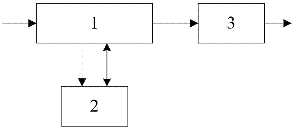
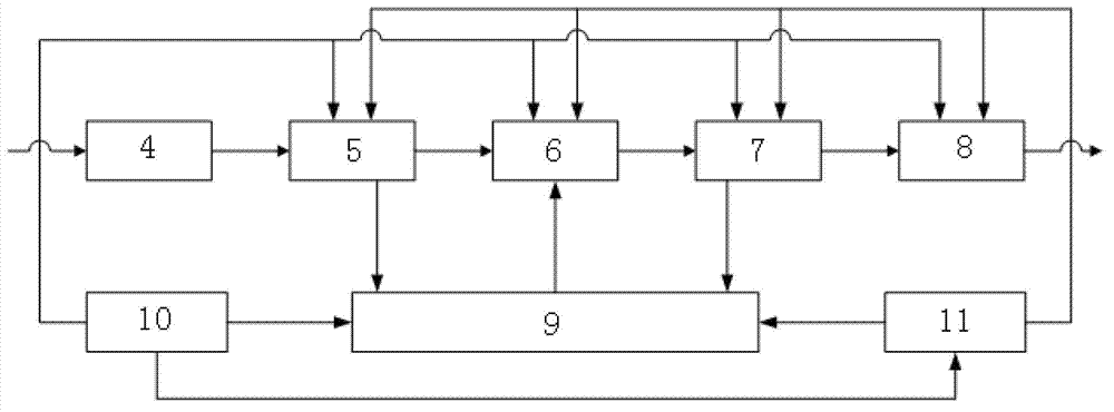
[0043] Examples of the invention figure 1 -5, an embedded system based on FPGA-based LCD signal to VGA signal is mainly constructed by FPGA module, SDRAM module and exclusion network module, which is characterized in that the FPGA module includes clock management module, reset module, LCD signal receiving Module, write FIFO module, SDRAM controller module, read FIFO module, FIFO controller module and VGA display module, LCD signal receiving module and write FIFO module are connected, write FIFO module and SDRAM controller module are connected, SDRAM controller module Connected to read FIFO module and SDRAM module respectively, FIFO controller module is connected to write FIFO module and read FIFO module respectively, read FIFO module is connected to VGA display module, clock management module is connected to reset module, write FIFO module, SDRAM respectively The controller module, read FIFO module, FIFO controller module, VGA display module and SDRAM module are connected, and ...

Embodiment 2

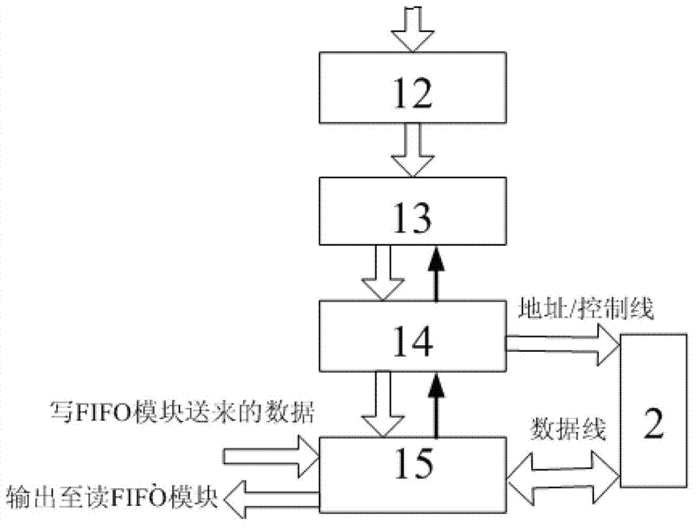
[0048] A method of using the above system to realize FPGA-based embedded LCD signal conversion to VGA signal. The input terminal of the FPGA module receives the LCD signal from the embedded system, including LCD field synchronization signal, LCD clock signal, LCD data valid signal and 24-bit LCD data signal, where the LCD field synchronization signal represents the end of the previous frame of image and the start of a new frame of image. The signal meets the LCD display timing; timing parameters (clock frequency, vertical blanking front shoulder, vertical blanking back shoulder, line The blanking front shoulder, line blanking back shoulder, etc.) have been defined in the embedded system kernel as a 1024x76820Hz signal. Since the received LCD signal resolution is 1024x768, the width is 24 bits, that is, a valid LCD signal has 768 lines, each line has 1024 pixels, a total of 1024x768 pixels. The FPGA module uses the LCD clock signal as the acquisition clock to collect 24-bit LCD d...


PUM


Abstract

The invention relates to a field programmable gate array-based (FPGA-based) realization method for converting a liquid crystal display (LCD) signal to a video graphics array (VGA) signal, which belongs to the technical field of the FPGA design, and a system is mainly established by an FPGA module, a synchronous dynamic random access memory (SDRAM) module and a register-packs network module. The FPGA module is used as a core of a conversion system, consists of a clock management module, a resetting module, an LCD signal receiving module, a writing first-in first-out (FIFO) module, an SDRAM controller module, a reading FIFO module, an FIFO controller module and a VGA display module and is realized through a Verilog hardware description language (HDL) code; the SDRAM module is a cache for processing the data of the FPGA module, and a controller of the SDRAM module is realized inside the FPGA module; and the exclusion network module is formed by register packs and used for converting a digital signal to an analog signal. The FPGA-based realization method has the advantages of low cost, short development period, low development risk, convenience in modification design and good confidentiality.

Description

Technical field [0001] The invention relates to a system and implementation method for converting embedded LCD signals into standard VGA interface signals based on FPGA, and belongs to the field of FPGA design technology. Background technique [0002] At present, the most commonly used display mode in embedded systems is LCD display. However, due to the inconsistent LCD interface, the expansion and maintenance of the system bring certain difficulties, and in some applications that require large-screen display, industrial-grade LCD The price is more expensive. As a general-purpose display device, CRT monitors and liquid crystal displays are widely used in our work and life. They have the advantages of large display area, rich colors, large carrying information, and unified VGA interface. If they are applied to embedded systems, they can significantly improve the visual effect of the product. [0003] With the continuous expansion of digital image processing applications, its real-...

Claims


Application Information

Patent Timeline
IPC IPC(8): G09G3/36G09G5/00
Inventor 袁东风徐祥桐徐加利纪洪亮孙文翟庆羽高凯
Owner SHANDONG UNIV
Why Eureka
Try Eureka