
Monolithic ceramic electronic component

A technology for electronic components and ceramics, applied in the field of laminated ceramic electronic components, can solve problems such as shortening the distance between internal electrodes, and achieve the effect of preventing the reduction of BDV

Active Publication Date: 2012-12-19
MURATA MFG CO LTD
View PDF4 Cites 3 Cited by
  • Summary
  • Abstract
  • Description
  • Claims
  • Application Information

AI Technical Summary

Problems solved by technology

In more detail, it has been found that the cause of this is that, when a dummy conductor exists in the outer layer portion where no internal electrode exists, the internal electrode overlapping with the dummy conductor is crushed by the dummy conductor at the time of pressing before firing. The presence of the presence of the need to press more than necessary, resulting in local shortening of the distance between the internal electrodes

Method used


Image

  • Monolithic ceramic electronic component
  • Monolithic ceramic electronic component
  • Monolithic ceramic electronic component

Examples


no. 1 Embodiment approach

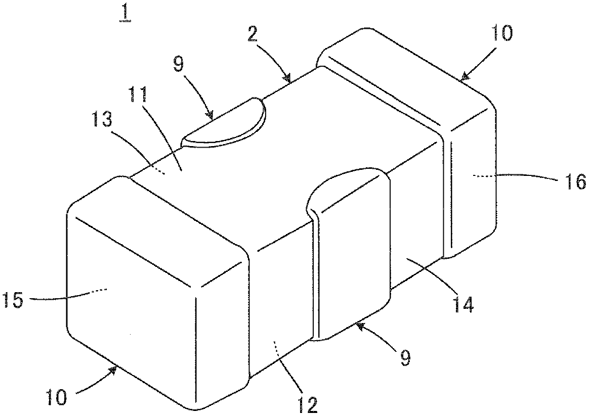
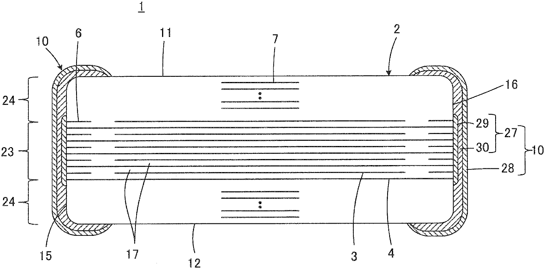
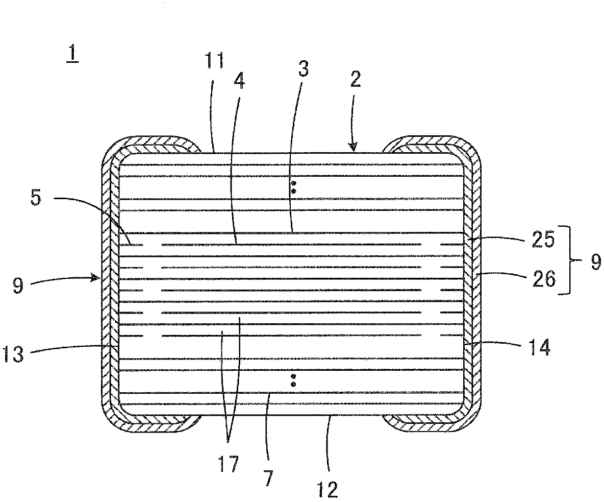
[0043] Figure 1 to Figure 7It is a figure for demonstrating the 1st Embodiment of this invention. The multilayer ceramic capacitor 1 of the first embodiment is a three-terminal type ceramic capacitor. A multilayer ceramic capacitor 1 includes a ceramic body 2; a first internal electrode 3 and a second internal electrode 4, a first inner layer dummy conductor 5 and a second inner layer dummy conductor 6 respectively arranged inside the ceramic body 2; Layer dummy conductor 7 , first external electrode 9 and second external electrode 10 arranged on the outer surface of ceramic body 2 . Hereinafter, the detailed structure of the multilayer ceramic capacitor 1 is divided into (1) a ceramic body, (2) internal electrodes, (3) inner layer dummy conductors, (4) outer layer dummy conductors, and (5) outer electrodes, respectively. (6) The production method will be described below.

[0044] (1) Ceramic body

[0045] The ceramic body 2 is approximately cuboid, and as its outer surfa...

no. 2 Embodiment approach

[0132] The second embodiment of the present invention is as Figure 8 shown. Figure 8 With image 3 corresponding figure. exist Figure 8 in, right with image 3 Elements corresponding to the elements shown are given the same reference numerals, and overlapping description thereof will be omitted.

[0133] In the multilayer ceramic capacitor 1a according to the second embodiment, the outer layer dummy conductors 7a are not formed to penetrate the ceramic green body 2 in the width direction, but are formed separately in the width direction.

no. 3 Embodiment approach

[0135] The third embodiment of the present invention is as Figure 9 as well as Figure 10 shown. Figure 9 With figure 1 corresponding figure, Figure 10 With image 3 corresponding figure. exist Figure 9 as well as Figure 10 in, right with figure 1 as well as image 3 Elements corresponding to the elements shown are given the same reference numerals, and repeated description thereof will be omitted.

[0136] In the multilayer ceramic capacitor 1b according to the third embodiment, the first external electrode 9b includes the base layer 25 and the upper layer 26, and is characterized in that the first side surface 13 and the second side surface 14 surrounding the ceramic body 2 also have a first main surface. 11 and the second main surface 12 are arranged.

[0137] In this embodiment, it is preferable to remove the ceramic layer 17 to be the main surface 11 and the main surface 12 by the aforementioned polishing step after firing, and to make the outer layer dummy...


PUM

PropertyMeasurementUnit
current densityaaaaaaaaaa

Abstract

The invention provides a monolithic ceramic electronic component. When an exposed portion of an inner electrode makes coating film separate out, in order to realize more stable coating growth, conditions exist that reliability of the monolithic ceramic electronic component such as BDV reduces when none outer-layer portion of any inner electrode forms a dummy conductor. Two or more outer-layer dummy conductors (7) are successively arranged at predetermined intervals in the height direction, thereby forming a plurality of outer-layer dummy groups (31). Given that an interval between the adjacent outer-layer dummy conductors (7) within each of the outer-layer dummy groups (31) is d and an interval between the adjacent outer-layer dummy groups (31) is g, g is greater than d. On that condition, the outer-layer dummy groups can be positioned satisfactorily apart away from each other, while plating deposition points are ensured. As a result, pressing of inner electrodes through the outer-layer dummy conductors (7) can be relieved, whereby the distance between the inner electrodes (3,4) can be prevented from being locally shortened and a reduction of BDV can be prevented.

Description

technical field [0001] The present invention relates to a laminated ceramic electronic component, and more particularly to a laminated ceramic electronic component including an external electrode including a plated film formed directly on the outer surface of a ceramic body. Background technique [0002] In recent years, the miniaturization of electronic equipment such as mobile phones, laptop computers, digital cameras, and digital audio equipment has been progressing. In these electronic equipment, multilayer ceramic electronic components that can be miniaturized and improved in performance are widely used. . [0003] Generally, a laminated ceramic electronic component includes a ceramic body having a plurality of laminated ceramic layers, internal electrodes formed inside the ceramic body, and external electrodes formed on the outer surface of the ceramic body. Furthermore, the multilayer ceramic electronic component is arranged on a conductive pad of a mounting substrat...

Claims


Application Information

Patent Timeline
Patent Type & Authority Applications(China)
IPC IPC(8): H01G4/228H01G4/30H01C1/14H01L41/04
CPCH01L41/273H01L41/29H01G4/30H01G4/228H01C1/14H01L41/0471H01L41/04H10N30/871H10N30/053H10N30/06H01G4/12
Inventor 樱谷昌弘山本重克
Owner MURATA MFG CO LTD
Learn More