Double-sided reusable templates for semiconductor substrates for fabrication of photovoltaic cells and microelectronic devices
A double-sided, template technology, applied in semiconductor devices, semiconductor/solid-state device manufacturing, photovoltaic power generation, etc.
- Summary
- Abstract
- Description
- Claims
- Application Information
AI Technical Summary
Problems solved by technology
Method used
Image

Examples
Embodiment Construction
[0027] Although the present invention is described with reference to specific embodiments, those skilled in the art can apply the principles discussed herein to other places and / or embodiments without undue experimentation.
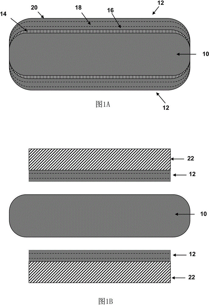
[0028] 1A and 1B show schematic cross-sectional views of the double-sided flat template 10 before and after the TFSS 12 is separated from both sides. As illustrated in FIG. 1A, through an epitaxial silicon growth process, in some embodiments, simultaneously, an epitaxially grown silicon layer is formed on both sides of the planar template and on top of the porous silicon layer 14 on the front and back surfaces of the template. The template may be made of a single crystal silicon wafer with a polished surface (although wafers and / or polycrystalline silicon wafers with an unpolished surface may also be used as templates). The wafer diameter may be in the range of about 150 to 450 mm, and the wafer thickness may be in the range of about 0.5 to 1 mm. Thicker wa...
PUM
 Abstract
Description
Claims
Application Information