Pcb with cavity and fabricating method thereof

A manufacturing method and cavity technology, which are applied in multilayer circuit manufacturing, printed circuit manufacturing, and mechanically removing conductive materials, etc., can solve the problems of narrowing the cavity design range and achieve the effect of precise control.

Active Publication Date: 2013-01-02
LG INNOTEK CO LTD
View PDF8 Cites 10 Cited by
  • Summary
  • Abstract
  • Description
  • Claims
  • Application Information

AI Technical Summary

Problems solved by technology

For this reason, the increase in production cost depends on the manufacturing cost of the punching jig P, so that the design range of the cavity is narrowed

Method used


Image

  • Pcb with cavity and fabricating method thereof
  • Pcb with cavity and fabricating method thereof
  • Pcb with cavity and fabricating method thereof

Examples


Embodiment Construction

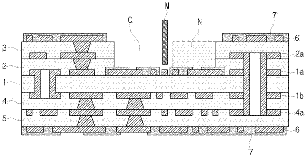
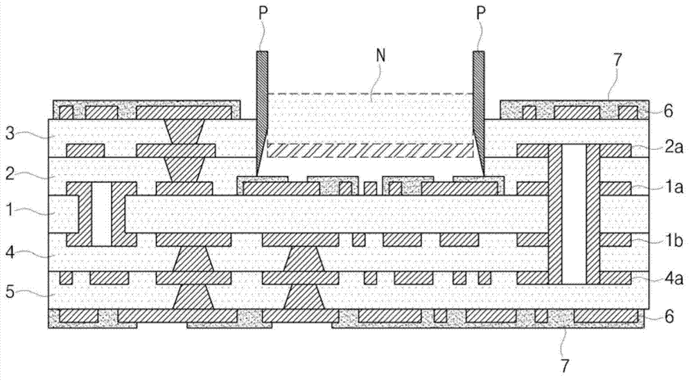
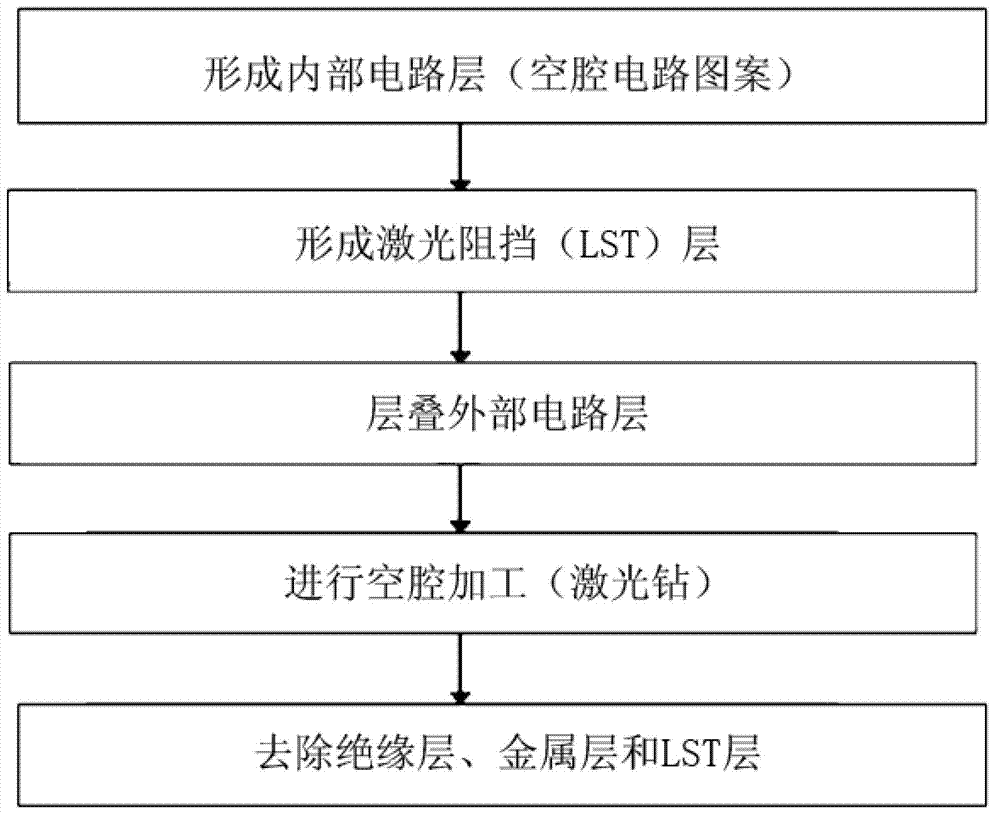
[0023] The present invention provides a method of manufacturing a printed circuit board with a cavity, in which a multilayer PCB is formed by a laser barrier, and then a cavity area is processed, whereby the processing freedom of the cavity can be improved and the circuit in the cavity can be protected .

[0024] For this, a basic circuit board is formed on the surface of the substrate, the basic circuit board is provided with an inner circuit layer including a cavity circuit pattern, and a laser blocking layer is partially formed on the cavity circuit pattern. Then, at least one outer circuit layer is formed on the basic circuit board, and a cavity region is formed on the upper portion of the laser blocking layer by removing the outer circuit layer.

[0025] Reference will now be made in detail to the exemplary embodiments of the present invention, examples of which are illustrated in the accompanying drawings, wherein like numerals refer to like elements throughout. Exempla...


PUM


Abstract

A fabricating method of a printed circuit board (PCB) with a cavity and a structure of the PCB fabricated by the method are provided. The method includes a first step of forming a base circuit board provided with an internal circuit layer having cavity circuit patterns on a surface of a substrate, a second step of forming a laser stopper layer on upper portions of the cavity circuit patterns, a third step of forming at least one external circuit layer on the base circuit board, and a fourth step of forming a cavity region by removing the external circuit layer on an upper portion of the laser stopper layer. Accordingly, in a fabricating method of a multi-layered PCB with a cavity, a laser stopper layer is formed on upper surfaces of cavity circuit patterns, so that it is possible to rapidly and precisely form the cavity, to precisely control the depth of the cavity and to have no influence on a circuit previously formed in the interior of the cavity.

Description

technical field [0001] The present invention relates to a method of manufacturing a printed circuit board (PCB) having a cavity formed in an area of ​​the PCB, and to a PCB structure manufactured by the method. Background technique [0002] A PCB is formed by printing a circuit pattern on an electrically insulating board with a conductive material such as copper. A PCB is a device used to mount electronic components. A PCB is a circuit board on which various electronic components are installed on a flat panel, and wires (wire patterns) are fixedly printed to connect these components, so that the components are densely mounted on the flat panel. PCBs are generally divided into single-layer PCBs and composite boards. For example, a multi-layer PCB is composed of multiple single-layers. [0003] Recently, system integration technology has made electronic products lighter, thinner, and smaller. Embedded PCB and PCB manufacturing technology with cavity achieve this effect. Th...

Claims


Application Information

Patent Timeline
Patent Type & Authority Applications(China)
IPC IPC(8): H05K3/04H05K3/46
CPCH05K3/0032H05K3/4697H05K1/186
Inventor 金亨钟俞在贤全振求朴峻秀李起龙
Owner LG INNOTEK CO LTD
Why Eureka
Try Eureka