Laser bonding temperature acquisition system for photoelectric device packaging and method for photoelectric device packaging

A technology of temperature acquisition system and photoelectric device, which is applied in the direction of thermometers using electric/magnetic elements directly sensitive to heat, electric devices, electric solid devices, etc., which can solve the problems of high design and manufacturing costs, complex structure of temperature acquisition devices, The temperature measurement effect is not ideal enough to achieve the effect of ensuring the packaging quality, good temperature detection effect, and simple structure

Active Publication Date: 2013-01-09
SHANGHAI UNIV
View PDF5 Cites 7 Cited by
  • Summary
  • Abstract
  • Description
  • Claims
  • Application Information

AI Technical Summary

Problems solved by technology

In order to measure the temperature of the glass frit bond, various temperature testing methods are applied to the hermetic sealing of OLED devices, but the te

Method used


Image

  • Laser bonding temperature acquisition system for photoelectric device packaging and method for photoelectric device packaging
  • Laser bonding temperature acquisition system for photoelectric device packaging and method for photoelectric device packaging
  • Laser bonding temperature acquisition system for photoelectric device packaging and method for photoelectric device packaging

Examples


Embodiment 1

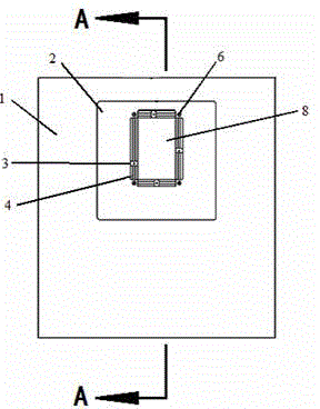
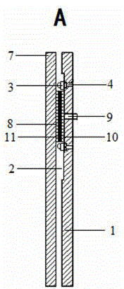
[0027] see figure 1 and figure 2 , a laser bonding temperature collection system for optoelectronic device packaging, including a temperature sensor and its positioning member, different temperature sensors are respectively arranged around the periphery of the glass substrate 10 used for optoelectronic device packaging, the temperature sensor can be set by the positioning member The position of the temperature collection point, so that different temperature sensors are arranged along the glass sealing strip 11 used for optoelectronic device packaging to carry out the temperature collection point layout, and the corresponding positions of the glass sealing strip 11 are respectively used for fixed-point temperature measurement, and the glass substrate 10 is fixedly installed on the support base plate 1, and there is an annular reserved gap between the outer edge of the glass substrate 10 and the notch edge of the positioning groove 2, and the positioning member is arranged in t...

Embodiment 2

[0039] The technical solution of this embodiment is basically the same as that of Embodiment 1, especially in that:

[0040] see Figure 4 , In this embodiment, an indicating scale 5 is also provided near the slideway 4, and the indicating scale 5 measures the current position of the indicating slide body on the slideway 4, and accurately positions the temperature sensor installed on the slideway. The indicator scale 5 of the sliding member can provide precise scales to facilitate precise positioning of the movement coordinates of the sliding body, thereby realizing more precise adjustment and positioning of the temperature sensor, and can accurately measure the temperature of different points of the glass sealing strip 11 .


PUM


Abstract

The invention discloses a laser bonding temperature acquisition system for photoelectric device packaging, which comprises a temperature sensor and locating elements thereof, wherein the locatingelements comprise a fixed-position locating element and a variable-position locating element; the temperature sensor, which is used for fixed point temperature measurement, of the fixed-position locating element is fixed onto a corresponding position corresponding to a glass sealing strip, and is used for testing fixed point temperature of the glass sealing strip; a movable part of the variable-position locating element is fixedly connected with other temperature sensors, so that the temperature sensors are limited to move along the periphery of the glass sealing strip; and temperature testing on different points of the glass sealing strip is realized through controlling positions of test points of the temperature sensor. The invention discloses a method for photoelectric device packaging, and through carrying out real-time fixed point temperature acquisition and real-time non-fixed point temperature acquisition on temperature of the glass sealing strip, the output power, the laser beam movement speed and the direction of a laser are controlled. According to the invention, the temperatures at different positions of glass material bonding parts can be simply and conveniently measured in real time, the structure is simple, and the efficiency is high.

Description

technical field [0001] The invention relates to a photoelectric device packaging technology, in particular to a temperature acquisition system and the use of the temperature acquisition system to collect laser bonding temperature to carry out a photoelectric device preparation process, which is used in the technical field of photoelectric device packaging. Background technique [0002] Organic light-emitting diode display technology has been valued due to its excellent luminous performance and wide application prospects. OLED has the advantages of high brightness, good color contrast, wide viewing angle, fast refresh rate and low energy consumption. However, the organic light-emitting layer and electrodes in the OLED device are very sensitive to oxygen and moisture in the surrounding environment, and will interact with it to degrade, thus greatly affecting the service life of the OLED device. The organic light-emitting layer and electrodes in the OLED device are separated f...

Claims


Application Information

Patent Timeline
IPC IPC(8): G01K7/02H01L51/56
Inventor 赖禹能葛军锋张建华黄元昊陈遵淼
Owner SHANGHAI UNIV
Why Eureka
Try Eureka