Transparent electrode manufacturing method, mask plate and equipment

A technology for transparent electrodes and manufacturing methods, applied in the fields of transparent electrode manufacturing methods, mask plates, and equipment, capable of solving problems such as uneven spacing and affecting display effects, achieving the effect of reducing spacing errors and improving display effects

Active Publication Date: 2014-11-05
TCL CHINA STAR OPTOELECTRONICS TECH CO LTD
View PDF1 Cites 0 Cited by
  • Summary
  • Abstract
  • Description
  • Claims
  • Application Information

AI Technical Summary

Problems solved by technology

The same situation also occurs during the etching process, resulting in different spacing between the transparent electrodes in the edge area of ​​the display area 110 and the transparent electrodes in the central area of ​​the display area 110, thereby affecting the display effect.

Method used


Image

  • Transparent electrode manufacturing method, mask plate and equipment
  • Transparent electrode manufacturing method, mask plate and equipment
  • Transparent electrode manufacturing method, mask plate and equipment

Examples


Embodiment Construction

[0021] The following description will be made in conjunction with the accompanying drawings and specific implementation manners.

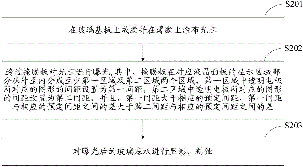
[0022] refer to figure 1 , figure 1 It is a flowchart of an embodiment of the transparent electrode manufacturing method of the present invention. The transparent electrode manufacturing method includes:

[0023] Step 201: forming a film on a glass substrate and coating a photoresist on the film.

[0024] A thin film is formed on a glass substrate by methods such as vacuum evaporation, sputtering, molecular beam evaporation or chemical evaporation, and then a photoresist is coated on the film by a photoresist coating machine.

[0025] Step 202: Exposing the photoresist through a mask.

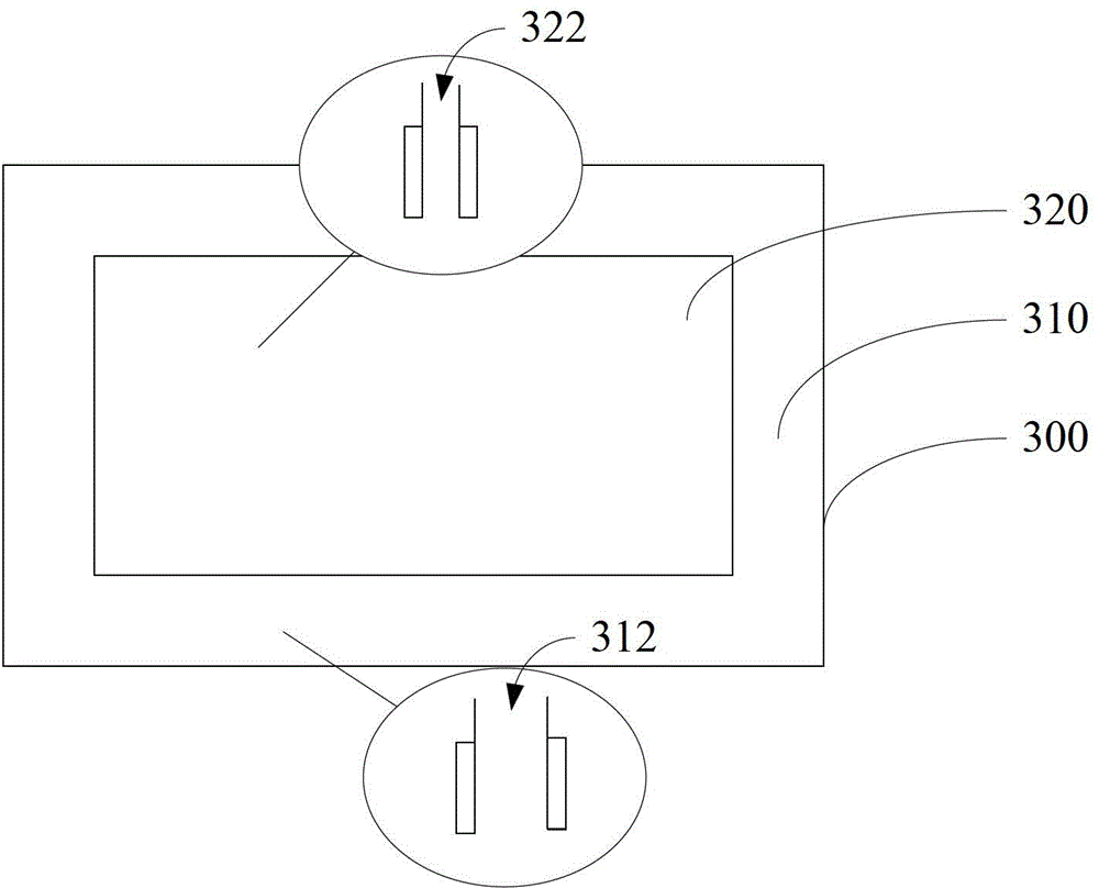
[0026] The glass substrate coated with the resistor is transported to the developing device, and the developing light source exposes the photoresist through the mask plate. Please also refer to image 3 , the mask plate is divided into at least two regions, th...


PUM


Abstract

A transparent electrode fabricating method and a mask plate. The method comprises the following steps: forming a film on a glass substrate and coating the film with a photoresist (S201); exposing the photoresist through the mask plate, which is divided at least into a first area (310) and a second area (320) from the outside to the inside in a display area part (300) of a corresponding liquid crystal panel, wherein an interval between patterns corresponding to a transparent electrode in the first area (310) is set to a first interval (312), an interval between patterns corresponding to a transparent electrode in the second area (320) is set to a second interval (322), the first interval (312) is larger than a corresponding predetermined interval, and the difference between the first interval (312) and the corresponding predetermined interval is larger than the difference between the second interval (322) and the corresponding predetermined interval (S202); and performing developing and etching (S203) on the glass substrate after exposure to form a transparent electrode on the glass substrate. In this mode, the error of an interval between transparent electrodes of the entire display area after formation can be reduced, thus improving the display effect.

Description

technical field [0001] The invention relates to the field of display technology, in particular to a transparent electrode manufacturing method, mask plate and equipment. Background technique [0002] At present, the manufacturing process of the transparent electrode of the substrate of the liquid crystal display is to form a film on the glass substrate and apply a photoresist on the film, and then expose the photoresist through a mask. Due to the shielding effect of the mask, the corresponding part of the pattern of the mask will not be exposed, and in the subsequent development process, the exposed photoresist will be washed away by the developer, and in the etching process, there is The photoresist-protected film will remain, forming the pattern of the transparent electrode. [0003] However, see figure 1 , in the substrate, the transparent electrodes are mainly distributed in the display area 110 (AA, Active Area), therefore, the display area 110 needs to keep more thin...

Claims


Application Information

Patent Timeline
Patent Type & Authority Patents(China)
IPC IPC(8): G02F1/1343G03F7/00
CPCG03F7/00G02F1/1343G02F1/13439G03F1/00G02F1/133388
Inventor 陈政鸿王醉
Owner TCL CHINA STAR OPTOELECTRONICS TECH CO LTD
Why Eureka
Try Eureka