

Atomic beam filling processing device
An atomic beam and carrier plate technology, applied in the field of workpiece surface processing, can solve the problems of inconvenient processing, bulky, complex ion beam generating device, etc., and achieve the effect of full filling processing
- Summary
- Abstract
- Description
- Claims
- Application Information
AI Technical Summary
Problems solved by technology
Method used
Image

Examples
Embodiment Construction
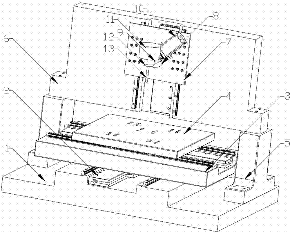
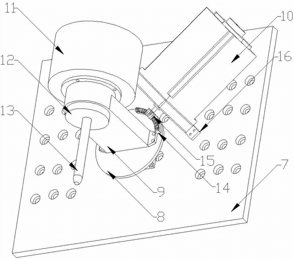
[0010] see figure 1 and 2 , the embodiment of the present invention is provided with a base 1, a linear motor 2, an X-axis bearing plate 3, a Y-axis bearing plate 4, a pillar 5, a beam 6, a Z-axis bearing plate 7, a rotating disc 8, a fixed seat 9, and a servo motor 10 , atomic beam generating device 11, atomic beam energy control device 12 and collimation device 13; the linear motor 2 is fixed on the base 1, and is fixedly connected with the X-axis carrier plate 3 through the connecting block, and the X-axis carrier plate 3 is connected with the The base 1 is connected by sliders and guide rails; between the Y-axis bearing plate 4 and the X-axis bearing plate 3, between the Z-axis bearing plate 7 and the beam 6 is connected by a linear motor 2 and a connecting block and adopts sliders and guide rails The pillars 5 are fixed on both ends of the base 1, the beam 6 is connected to the pillars 5, the rotating disk 8 is equipped with an arc-shaped rack 14 and is fixed on the Z-ax...
PUM
 Abstract
Description
Claims
Application Information