Single-layer externally hanging touch panel and manufacturing method thereof and liquid crystal display
A touch screen and plug-in technology, which is applied in the directions of instruments, optics, and electrical digital data processing, etc., can solve problems such as large steepness, pollution of the touch screen in the sputtering equipment chamber, and difficult process of single-layer plug-in touch screen, so as to avoid pollution Effect
- Summary
- Abstract
- Description
- Claims
- Application Information
AI Technical Summary
Problems solved by technology
Method used
Image

Examples
Embodiment 1
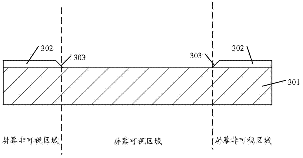
[0077] This embodiment provides a single-layer external touch screen manufacturing method, such as Figure 3(1)~3(11) As shown, the manufacturing method of the process specifically includes:
[0078] Step A, coating a layer of BM material on the glass substrate 301, and then performing photoetching treatment on the layer of BM material to form a BM Pattern 302 covering the non-visible area of the screen, as shown in Figure 3 (1), the BM pattern The position close to the visible area of the screen on the Pattern 302 has a slope-shaped first step difference part 303;
[0079] In step B, the glass substrate 301 of the BM Pattern 302 is coated with a layer of transparent and insulating resin-type material, the baking temperature of the resin-type material is lower than the lowest temperature that causes the volatilization of the BM material, and then the layer of resin-type material is Carry out baking, form the first film layer 304, as shown in Figure 3 (2), the thickness of...
Embodiment 2
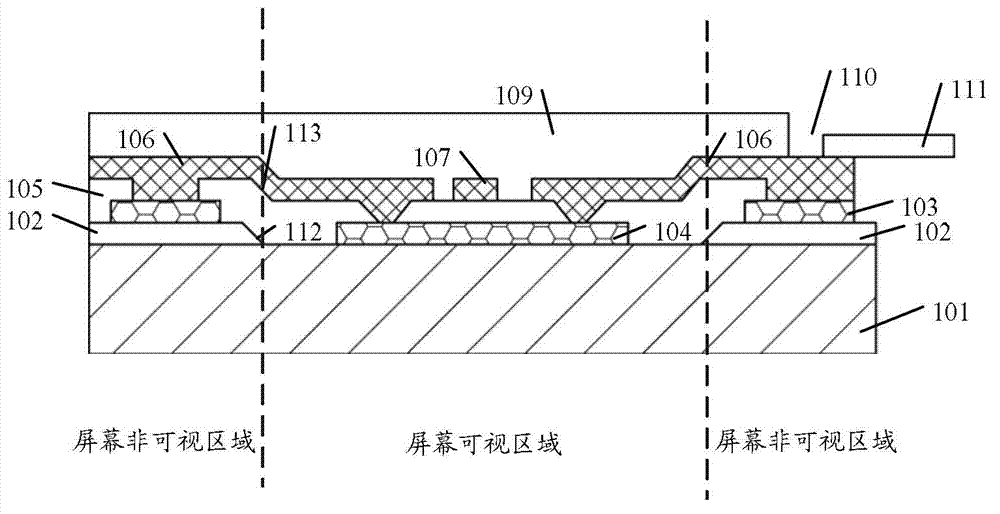
[0106] This embodiment provides a single-layer external touch screen, such as Figure 4 As shown, it includes: substrate 401, BM Pattern 402, level difference part 403, first film layer 404, first slope-shaped part 405, isolation pad 406, metal trace 407, metal bridge 408, second film layer 409, via hole 410, the first hollow pattern 411 (not shown in the figure), the second slope part 412, the intermittent conductive wiring 413, the continuous conductive wiring 414, the third film layer 415, the second hollow pattern 416, the flexographic printing circuit board 417;
[0107] Among them, the substrate 101 is made of glass material; it covers the entire screen area; it is used to carry the functional units that constitute the entire single-layer external touch screen;
[0108] BM Pattern 402 is made of BM material (resin material containing black dye); it is formed on the substrate 401 and is located in the non-visible area of the screen; it is used to block the light in the...
Embodiment 3
[0122] This embodiment provides a liquid crystal display, such as Figure 5 As shown, the display includes: a single-layer external touch screen 501, an OC layer 502, a TFT-LCD liquid crystal display 503; wherein,
[0123] The single-layer external touch screen 501 has the single-layer external touch screen structure provided by the present invention;
[0124] The OC layer 502 adopts optical glue OCA, which is coated on the outer surface of the third film layer in the single-layer external touch screen 501;
[0125] The TFT-LCD liquid crystal display 503 is bonded to the single-layer external touch screen 501 through the OC layer 502 .
PUM
 Abstract
Description
Claims
Application Information
 - Generate Ideas
- Intellectual Property
- Life Sciences
- Materials
- Tech Scout
- Unparalleled Data Quality
- Higher Quality Content
- 60% Fewer Hallucinations
Browse by: Latest US Patents, China's latest patents, Technical Efficacy Thesaurus, Application Domain, Technology Topic, Popular Technical Reports.
© 2025 PatSnap. All rights reserved.Legal|Privacy policy|Modern Slavery Act Transparency Statement|Sitemap|About US| Contact US: help@patsnap.com