
Method for improving etched via bottom critical dimension of 40 nm dual damascene structure

A technology of etching gas and grooves, applied in the direction of electrical components, semiconductor/solid-state device manufacturing, circuits, etc., can solve problems such as unfavorable formation, bending, affecting electrical properties and yield, and achieve the effect of increasing critical dimensions

Inactive Publication Date: 2013-01-16
SHANGHAI HUALI MICROELECTRONICS CORP
View PDF4 Cites 6 Cited by
  • Summary
  • Abstract
  • Description
  • Claims
  • Application Information

AI Technical Summary

Problems solved by technology

[0002] In the 40nm 1XDD (one-time design specification) double-damascene structure metal hard mask, the ultra-low dielectric insulating layer (Ultra-low dielectric constant, ULK) in the AIO (all in one) etching process, due to the ultra-low k The dielectric insulating layer contains a large amount of carbon doping and porous structure, and the plasma is easy to cause damage to the ultra-low-k dielectric insulating layer, resulting in specific defects such as kinks and bending (kink / bowing), which is not conducive to the potential barrier and Cu follow-up. fill and affect electrical and yield
In order to reduce the damage to the ultra-low-k dielectric insulating layer, in general, in the step of opening the Via after the trench etching of the ultra-low-k dielectric insulating layer, the industry generally adopts the relative reaction to generate a deposit (Polymer-depo) Dense gases (such as C 4 f 8 ) mainly low-pressure and high-frequency plasma etching steps, but a common adverse effect caused by this is that the critical dimension (Via Bottom CD, VBCD) at the bottom of the final via hole is too small to be unfavorable for formation

Method used


Image

  • Method for improving etched via bottom critical dimension of 40 nm dual damascene structure
  • Method for improving etched via bottom critical dimension of 40 nm dual damascene structure
  • Method for improving etched via bottom critical dimension of 40 nm dual damascene structure

Examples


Embodiment Construction

[0023] According to the unique characteristics of the ultra-low-k dielectric insulating layer, the present invention proposes a method that can not only protect the sidewall of the low-k dielectric insulating layer, but also increase the critical dimension of the bottom of the through hole.

[0024] The following examples illustrate the improvement methods provided by the present invention in further detail in order to better understand the content created by the present invention, but the content of the examples does not limit the scope of protection created by the present invention.

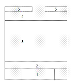
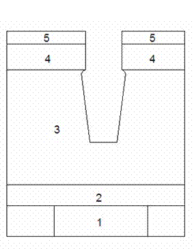
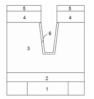
[0025] The overall improvement of the key dimensions of the 40nm double damascene structure to etch the bottom of the through hole includes three parts: a trench etching step, a step of forming a sidewall protection layer of an ultra-low-k dielectric insulating layer, and a step of forming a through hole that exposes the metal layer.

[0026] Such as figure 1 with 2 As shown, the trench etching step is...


PUM


Abstract

The invention provides a method for improving etched via bottom critical dimension (VBCD) of a 40 nm dual damascene structure. The method comprises the following steps: etching a groove, forming a protective layer of side walls of a ULK (Ultra-low dielectric constant) layer, and forming vias of an exposed metal layer. According to the method provided by the invention, the side walls of the ULK layer can be protected, and the VBCD can be enlarged in the step for etching the groove in the 1*DD AIO (all in one) process.

Description

Technical field [0001] The invention relates to the technical field of semiconductor preparation and etching, and in particular to a method for improving the key dimensions of the bottom of an etching through hole in a 40nm 1XDD (double design specification) double damascene structure. Background technique [0002] In the 40nm 1XDD (double design specification), the ultra-low dielectric constant (ULK) of the metal hard mask of the double Damascus structure is used in the AIO (all in one) etching process, due to the ultra-low k The dielectric insulating layer contains a large amount of carbon doping and multi-vacancy structure. Plasma is easy to damage the ultra-low-k dielectric insulating layer and cause specific defects such as kink / bowing, which is not conducive to the potential barrier and Cu follow-up Filling affects electrical properties and yield. In order to reduce the damage to the ultra-low-k dielectric insulating layer, in general, in the step of opening the Via after ...

Claims


Application Information

Patent Timeline
Patent Type & Authority Applications(China)
IPC IPC(8): H01L21/768
Inventor 黄君张瑜盖晨光
Owner SHANGHAI HUALI MICROELECTRONICS CORP
Learn More