A flip-chip light-emitting diode structure and manufacturing method thereof
A technology of light-emitting diodes and manufacturing methods, applied to electrical components, circuits, semiconductor devices, etc., can solve problems such as chip short circuits, achieve the effects of avoiding short circuits, protecting side walls, and improving reliability and yield
- Summary
- Abstract
- Description
- Claims
- Application Information
AI Technical Summary
Problems solved by technology
Method used
Image
Examples
Embodiment 1
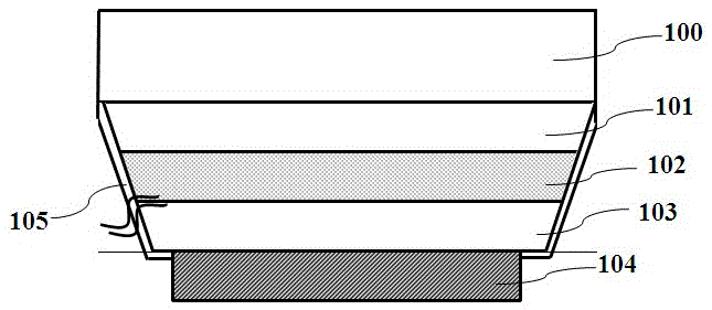
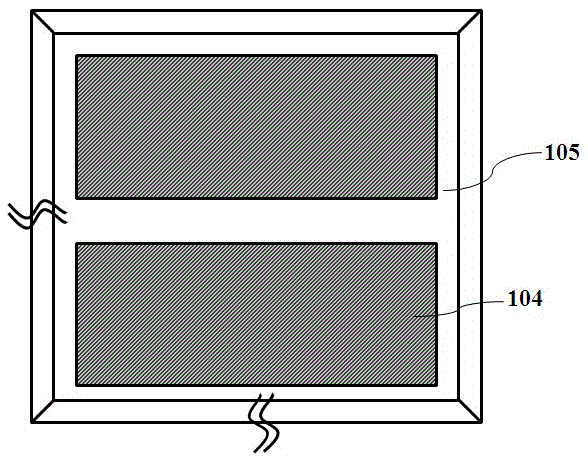
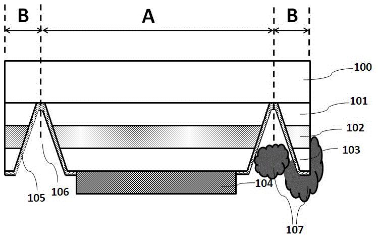
[0042] like image 3 and 4 The gallium nitride-based flip-chip light-emitting diode shown includes: a growth substrate 100, an N-type layer 101, a light-emitting layer 102, a P-type layer 103, a metal electrode 104, an insulating layer 105, a V-shaped opening structure 106, and an epitaxial body layer A with barrier structure B.
[0043]Specifically, the growth substrate 100 in the above GaN-based flip-chip light-emitting diode structure is a sapphire substrate; the epitaxial layer is formed on the light-emitting layer 102, wherein the epitaxial layer includes an N-type layer 101, a light-emitting layer 102, and a P-type layer 103 in sequence. The V-shaped opening structure 106 is located above the edge of the epitaxial layer and extends to the surface of the growth substrate 100, so that part of the sidewall of the epitaxial layer and part of the substrate surface are exposed, thereby dividing the epitaxial layer into epitaxial body layer A and The barrier structure B, beca...
Embodiment 2
[0045] like Figure 5~9 The schematic cross-sectional schematic diagram of the manufacturing process of the flip-chip light-emitting diode structure shown, specifically:
[0046] like Figure 5 As shown, a growth substrate 100 is provided first. In this embodiment, the growth substrate 100 is selected from sapphire to form an epitaxial substrate of a GaN-based flip-chip light-emitting diode; however, it should be recognized that the growth substrate 100 can also be Silicon carbide or gallium nitride or silicon or other substrates;
[0047] like Figure 6 As shown, an epitaxial layer is grown on a growth substrate 100, and the epitaxial layer includes an N-GaN layer 101, a light-emitting layer 102, and a P-GaN layer 103 in sequence. Furthermore, a GaN buffer layer can be grown on the growth substrate first, and then grown Epitaxial layer for better lattice quality;
[0048] like Figure 7 As shown, the chip size is defined by the ICP etching process, and the V-shaped openi...
Embodiment 3
[0052] like Figure 10 As shown, the difference from Embodiment 1 is that in this embodiment, a reflective layer 108 is formed before the V-shaped opening structure 106 is formed on the epitaxial layer. The reflective layer 108 can be a reflective metal layer or a distributed Bragg reflective layer or a full As for the azimuth reflective layer, the reflective layer 108 in this embodiment is preferably a reflective metal layer, and the reflective metal layer may include Ni, Pt, Ag, Al, or Rh.
PUM
 Abstract
Description
Claims
Application Information


