
Formation method of CMOS transistor

A transistor and gas technology, applied in the field of CMOS transistor formation, can solve the problems of metal gate quality degradation, sidewall concave, CMOS transistor performance degradation, etc., to achieve the effects of flat sidewall surface, improved performance, and prevention of accumulation

Active Publication Date: 2015-11-25
SEMICON MFG INT (SHANGHAI) CORP
View PDF4 Cites 0 Cited by
  • Summary
  • Abstract
  • Description
  • Claims
  • Application Information

AI Technical Summary

Problems solved by technology

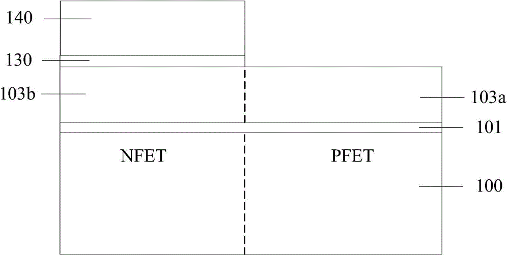
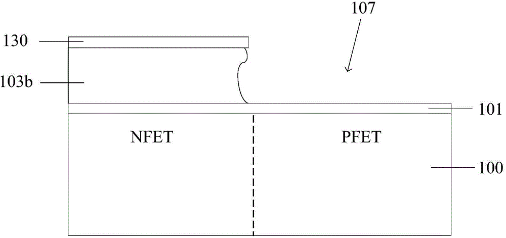
The dummy gate 103a and the dummy gate 103b are actually an integral structure connected together. When the continuous wave plasma etching process removes the dummy gate 103a, the sidewall of the dummy gate 103b will be partially etched at the same time, resulting in a dummy gate 103b has a sidewall concave problem (bowing issue), that is, the sidewall of the dummy gate 103b cannot be kept straight, and there is a situation in which it is recessed into the dummy gate 103b, such as image 3 shown
[0007] When the side wall of the gate 103b has a concave problem, on the one hand, it will increase the difficulty of filling the subsequent opening 107, and on the other hand, it will cause the quality of the metal gate formed by the subsequent filling to decline, thereby resulting in the performance degradation of the CMOS transistor.
Moreover, after filling the opening 107 to form a metal gate, when continuing to remove the dummy gate 103b, there will be a problem that the dummy gate 103b cannot be completely removed, causing the performance of the CMOS transistor to degrade again.
[0008] For this reason, a new method for forming CMOS transistors is needed to avoid the problem of concave sidewalls during the removal of dummy gates during the formation of CMOS transistors.

Method used


Image

  • Formation method of CMOS transistor
  • Formation method of CMOS transistor
  • Formation method of CMOS transistor

Examples


Embodiment Construction

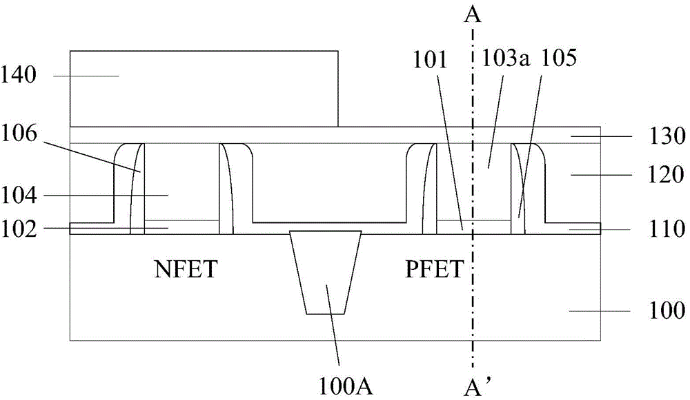
[0038] In a CMOS transistor using a high-K dielectric layer-metal gate (HKMG), the work function metal materials used in the NMOS transistor and the PMOS transistor that make up the CMOS transistor are usually different, so the dummy gates of the NMOS transistor and the PMOS transistor need to be removed separately . However, as described in the background art, when the first dummy gate and the second dummy gate connected together are etched in the existing CMOS transistor formation method, after the first dummy gate is removed, the second dummy gate is prone to appear The sidewall concave problem causes the performance of the finally formed CMOS transistor to degrade.

[0039] To this end, the present invention provides a new method for forming a CMOS transistor, which uses a first pulse plasma etching process to remove part of the thickness when etching the first dummy gate and the second dummy gate that are connected together. the first dummy gate, and expose part of the s...


PUM


Abstract

A formation method of a CMOS transistor comprises the steps of providing a semiconductor substrate, wherein the semiconductor substrate comprises a first area, a second area and a shallow trench isolation structure; forming a first pseudo gate on the first area and forming a second pseudo gate on the second area, wherein the first and second pseudo gates are connected along a length direction of the shallow trench isolation structure; using a first pulse plasma etching technology to remove the first pseudo gate of partial thickness and exposing a part of the side wall of the second pseudo gate; forming a protection layer to cover the exposed side wall of the second pseudo gate; after the protection layer is formed, adopting a second pulse plasma etching technology to remove the first pseudo gate of residual thickness until an opening is formed; adopting a metal material to fill the opening. By the formation method of the CMOS transistor, the performance of the formed CMOS transistor is improved.

Description

technical field [0001] The invention relates to the field of semiconductor manufacturing, in particular to a method for forming a CMOS transistor. Background technique [0002] With the continuous development of semiconductor manufacturing technology, the critical dimension (Critical Dimension, CD) of semiconductor devices in integrated circuits is getting smaller and smaller. In order to solve a series of problems caused by small-sized devices, gates of high dielectric constant (k) materials The technology of combining dielectric layer and metal gate (metalgate) is introduced into the manufacturing process of CMOS transistors. [0003] In order to avoid the influence of the metal material of the metal gate on other structures of the CMOS transistor, the gate stack structure of the metal gate and the high-k gate dielectric layer is usually fabricated by a gate-last process. In this process, a dummy gate made of polysilicon and other materials is first formed at the position...

Claims


Application Information

Patent Timeline
Patent Type & Authority Applications(China)
IPC IPC(8): H01L21/8238
Inventor 张海洋尚飞
Owner SEMICON MFG INT (SHANGHAI) CORP
Learn More