Forming method of dielectric layer

A dielectric layer and semiconductor technology, used in electrical components, semiconductor/solid-state device manufacturing, circuits, etc., can solve problems such as changes in the capacitance value of ultra-low-k dielectric layers, prevent k-value drift and large changes in capacitance, and avoid dielectric Influence of electric constant, effect of guaranteeing stability and reliability

Active Publication Date: 2013-01-23
SEMICON MFG INT (SHANGHAI) CORP
View PDF6 Cites 0 Cited by
  • Summary
  • Abstract
  • Description
  • Claims
  • Application Information

AI Technical Summary

Problems solved by technology

[0008] In the prior art, when metal wiring or conductive plugs are formed in the ultra-low-k dielectric layer, the dielectric constant k value of the ultra-low-k dielectric layer will drift (k value becomes larger), resulting in a change in the capacitance value of the ultra-low-k dielectric layer changes, causing serious problems in the stability and reliability of semiconductor devices

Method used


Image

  • Forming method of dielectric layer
  • Forming method of dielectric layer
  • Forming method of dielectric layer

Examples


no. 1 example

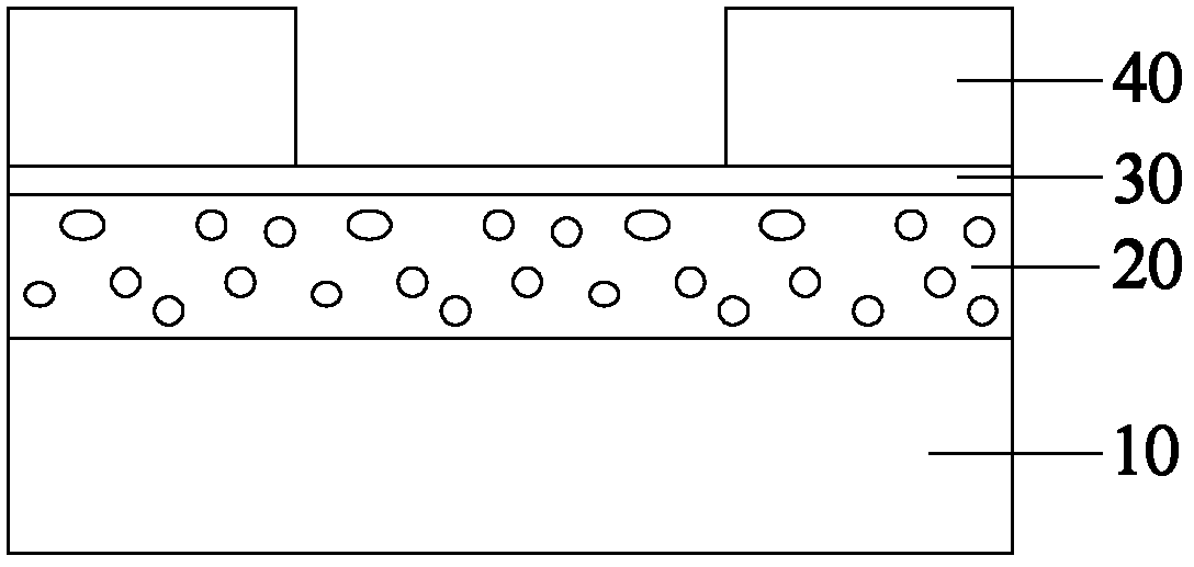
[0031] Figure 6 to Figure 11 It is a schematic diagram of the first embodiment of forming a semiconductor device including an ultra-low-k dielectric layer according to the present invention (taking the formation of a metal wiring layer as an example). Such as Figure 6 As shown, a semiconductor substrate 100 is provided, and structures such as transistors, capacitors, and metal wiring layers are usually formed on the semiconductor substrate 100 through previous processes.

[0032] Because in the process of fabricating the metal wiring in this embodiment, the thickness of the dielectric layer to be formed is 2400 angstroms to 3000 angstroms. Therefore, using the method of this embodiment, the first layer of dielectric material 200a is first formed on the semiconductor substrate 100 by chemical vapor deposition, and the thickness of the first layer of dielectric material 200a is 800 angstroms to 1000 angstroms. Then, a first carbon treatment 300a is performed on the first lay...

no. 2 example

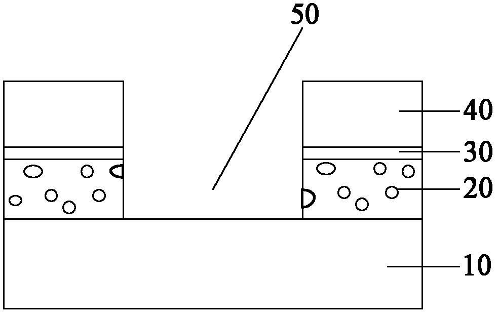
[0046] Figure 12 to Figure 19 It is a schematic diagram of a second embodiment of forming a semiconductor device including an ultra-low-k dielectric layer according to the present invention (taking the formation of a conductive plug of a dual damascene structure as an example). Such as Figure 12 As shown, a semiconductor substrate 1000 is provided, and structures such as transistors, capacitors, and metal wiring layers are usually formed on the semiconductor substrate 1000 through previous processes;

[0047] Because in the process of manufacturing the conductive plug of the dual damascene structure in this embodiment, the thickness of the dielectric layer to be formed is 3200 angstroms to 4000 angstroms. Therefore, using the method of this embodiment, the first layer of dielectric material 2000a is first formed on the semiconductor substrate 1000 by chemical vapor deposition, and the thickness of the first layer of dielectric material 2000a is 800-1000 angstroms. Then, th...


PUM

PropertyMeasurementUnit
thicknessaaaaaaaaaa
thicknessaaaaaaaaaa
thicknessaaaaaaaaaa

Abstract

A forming method of a dielectric layer comprises the following steps of: providing a semiconductor substrate; forming the dielectric layer on the semiconductor substrate, wherein the dielectric layer is formed by at least twice depositions, and a preset thickness is deposited every time; and carrying out carbon treatment on the dielectric layer after each deposition. According to the invention, k value drift and great capacitance change of the ultralow-k dielectric layer are effectively prevented, and stability and reliability of a semiconductor device are guaranteed.

Description

technical field [0001] The invention relates to a semiconductor manufacturing process, in particular to a method for forming a dielectric layer. Background technique [0002] At present, in the back-end process of semiconductor manufacturing, in order to connect various components to form an integrated circuit, metal materials with relatively high conductivity such as copper are usually used for wiring, that is, metal wiring. Whereas, conductive plugs are usually used for connection between metal wirings. The structures used to connect the active regions of semiconductor devices to other integrated circuits are typically conductive plugs. Existing conductive plugs are formed through a via process or a dual damascene process. [0003] In the existing process of forming copper wiring or conductive plugs, trenches or via holes are formed by etching the dielectric layer, and then conductive substances are filled in the trenches or via holes. However, when the feature size rea...

Claims


Application Information

Patent Timeline
Patent Type & Authority Applications(China)
IPC IPC(8): H01L21/3105
Inventor 邓浩张彬
Owner SEMICON MFG INT (SHANGHAI) CORP
Why Eureka
Try Eureka