A method for producing a deposit and a deposit on a surface of a silicon substrate
A silicon substrate and deposit technology, applied in gaseous chemical plating, coatings, electrical components, etc., can solve problems such as weak passivation, and achieve the effects of good passivation properties, short purge time, and good passivation effect
- Summary
- Abstract
- Description
- Claims
- Application Information
AI Technical Summary
Problems solved by technology
Method used
Image
Examples
Embodiment 1
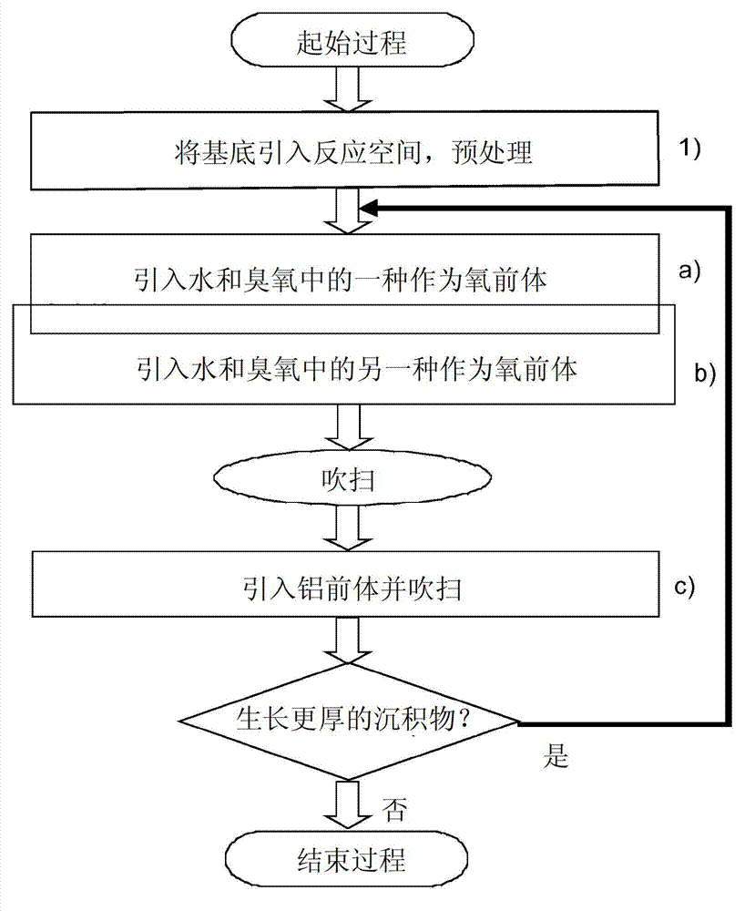
[0073] In this example, according to figure 2 In the illustrated embodiment of the invention, a passivation deposit is formed on the surface of a single crystal silicon substrate (eg, a single crystal wafer).
[0074] Condition the substrate before introducing it into the reaction space. In this step, possible impurities were removed from the exposed surface of the monocrystalline silicon substrate by etching in a 1% HF solution for 30 s, followed by rinsing in distilled water.
[0075] After conditioning, the substrate was inserted into the reaction space of a P400ALD batch unit (obtained from Beneq OY, Finland). The substrate is positioned within the reaction space such that the surface of the single crystal silicon substrate is exposed to the reaction environment.
[0076]After the preparation of loading the substrate into the ALD unit, the reaction space of the ALD unit is pumped down to negative pressure and a continuous carrier gas flow is set to achieve a process pre...
Embodiment 2
[0081] In this example, according to figure 1 In the illustrated embodiment of the invention, a passivation deposit is formed on the surface of a single crystal silicon substrate (eg, a single crystal wafer).
[0082] Condition the substrate before introducing it into the reaction space. In this step, possible impurities were removed from the exposed surface of the monocrystalline silicon substrate by etching in a 1% HF solution for 30 s, followed by rinsing in distilled water.
[0083] After conditioning, the substrate was inserted into the reaction space of a P400ALD batch unit (obtained from Beneq OY, Finland). The substrate is positioned in the reaction space such that the surface of the single crystal silicon substrate is exposed to the reaction environment.
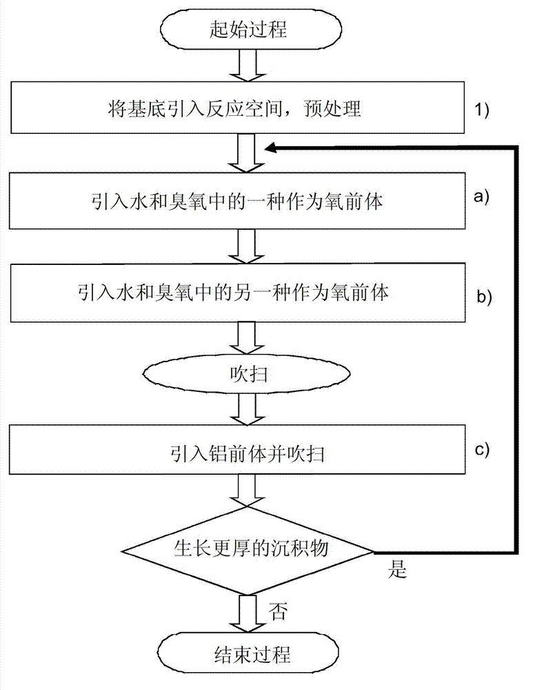
[0084] After the preparation of loading the substrate into the ALD unit is completed, the reaction space of the ALD unit is pumped down to negative pressure, and a continuous carrier gas flow is set to achieve a p...
PUM
 Abstract
Description
Claims
Application Information


