

Cutting method for MEMS wafer
A cutting method, wafer technology, applied in the fields of technology for producing decorative surface effects, decorative arts, gaseous chemical plating, etc.
- Summary
- Abstract
- Description
- Claims
- Application Information
AI Technical Summary
Problems solved by technology
Method used
Image

Examples
Embodiment Construction
[0023] Specific embodiments of the present invention will be described in detail below in conjunction with the accompanying drawings.
[0024] The cutting method of the MEMS wafer that the present invention relates to, it comprises the following steps:
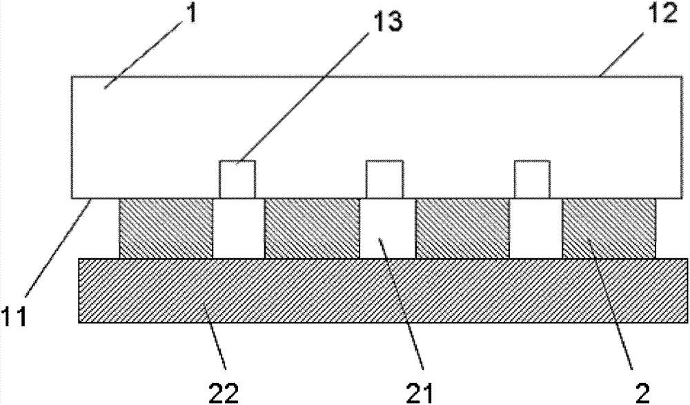
[0025] The first step, to protect the MEMS structure,
[0026] Such as figure 1 As shown, the front side 11 of the MEMS wafer 1 is provided with MEMS structures 13 . Paste the first film 2 with holes 21 on the front surface of the wafer 11. The holes 21 correspond to the MEMS structures 13 one by one, and the size of the holes 21 is slightly larger than the MEMS structures 13. The MEMS structure corresponds to the middle position of the holes 21. The complete second membrane 22 is pasted on the top of the first membrane 2, thereby forming a closed protection space at the hole 21, and the MEMS structure 13 is effectively protected.
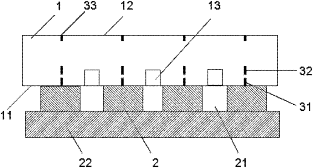
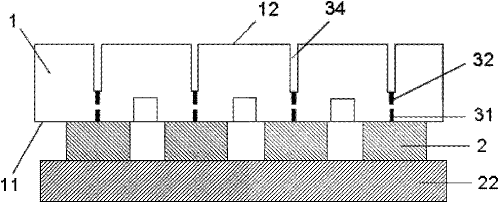
[0027] In the second step, wafer thinning,
[0028] The backside 12 of the wafer 1 is thinn...
PUM
| Property | Measurement | Unit |
|---|---|---|
| depth | aaaaa | aaaaa |
| width | aaaaa | aaaaa |
| depth | aaaaa | aaaaa |
Abstract
Description
Claims
Application Information