A packaging structure of a low-k chip and a manufacturing method thereof

A chip packaging structure, low-k technology, applied in semiconductor/solid-state device manufacturing, electrical components, electrical solid-state devices, etc., can solve problems such as fragmentation and integrated circuit failure

Active Publication Date: 2014-03-26
SEMICON MFG INT (SHANGHAI) CORP
View PDF4 Cites 3 Cited by
  • Summary
  • Abstract
  • Description
  • Claims
  • Application Information

AI Technical Summary

Problems solved by technology

During the welding process (Bonding), the connection structure will easily cause the dielectric layer 6 of the ultra-low dielectric constant material in the metal layer to break due to the stress between the solder ball and the metal layer, and then cause the failure of the integrated circuit

Method used


Image

  • A packaging structure of a low-k chip and a manufacturing method thereof
  • A packaging structure of a low-k chip and a manufacturing method thereof

Examples


Embodiment 1

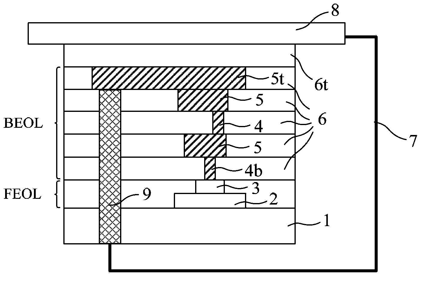
[0043] Embodiment 1. The step of forming TSV holes is performed before the FEOL process. That is, the TSV holes are pre-formed on the substrate before the FEOL process, and the TSV holes are gradually connected to the topmost connection line in the metal layer during the subsequent process. The process includes:

[0044] Provide the substrate before the FEOL process;

[0045] forming TSV holes in the substrate;

[0046] forming a chip on the substrate by FEOL process;

[0047] The metal layer is formed by a BEOL process, and the TSV hole extends to the topmost connection line in the metal layer and is electrically connected to the topmost connection line.

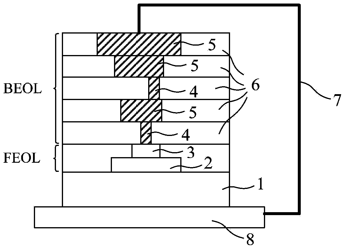
[0048] Please refer to figure 2 The packaging structure of the low-k chip of the present invention is shown. The specific formation process of the TSV holes mentioned above in the first embodiment is as follows.

[0049] First, a substrate 1 is provided.

[0050] Then, the existing TSV hole 9 forming method can be u...

Embodiment 2

[0054] Embodiment 2. The step of forming TSV holes is performed during the FEOL process. That is, TSV holes are formed on the substrate during the FEOL process, and the TSV holes are gradually connected to the topmost connection line in the metal layer in the subsequent process.

[0055] Because the FEOL process consists of multiple processes, such as the formation of STI (Shallow Trench Isolation, shallow trench isolation) in the substrate 1, the formation of wells, and the gate structure in CMOS (Complementary Metal Oxide Semiconductor, Complementary Metal Oxide Semiconductor) devices The formation of the source / drain region and so on. In the second embodiment, the step of forming the TSV hole 9 may be performed between these steps in the FEOL process as required. The formed TSV hole 9 penetrates the substrate 1 . In the subsequent process, it is necessary to pay attention to the treatment of the formed TSV hole 9. For example, when forming an interlayer dielectric layer, ...

Embodiment 3

[0056] Embodiment 3. The step of forming TSV holes is performed after the FEOL process and before the BEOL process. That is, after the FEOL process is completed and before the BEOL process is started, TSV holes are formed on the substrate and the chip layer formed by FEOL, and the TSV holes are gradually connected to the topmost connection line in the metal layer during the subsequent process.

[0057] Take the manufacture of CMOS devices as an example, and refer to figure 2 . First, a chip 2 is formed on the substrate 1. The chip 2 is composed of CMOS devices, which include NMOS (N-Metal-Oxide-Semiconductor, N-type metal oxide semiconductor) and PMOS (P-Metal-Oxide-Semiconductor, P-type Metal Oxide Semiconductor) devices, NMOS includes its gate structure and source / drain, similarly, PMOS includes its gate structure and source / drain. In the structure formed after the FEOL process is completed, there are generally structures such as an interlayer dielectric layer deposited o...


PUM


Abstract

The invention discloses a packaging structure of a low-k chip. The packaging structure comprises a substrate, a metallic layer, a TSV, and a bonding pad. A chip is formed on the substrate. The metallic layer is formed on the chip and comprises multiple vias and multiple connecting lines which are mutually and electrically connected, and dielectric layers produced by material with an ultra low-k and filled around the vias and the connecting lines. A dielectric layer at the top covers a connecting line at the top in the metallic layer. The TSV is arranged from the connecting line at the top in the metallic layer to the bottom of the substrate and passes through the substrate. The bonding pad is disposed on the dielectric layer at the top of the metallic layer and is electrically connected with the one end of the TSV on the bottom of the substrate through a metallic line. In the packaging structure, the connecting line at the top is directly guided to the bottom of the substrate via the TSV and then is connected with a bonding gasket through one end of the TSV on the bottom of the substrate without material with an ultra low-k. As a result, the crack of the dielectric layer with an ultralow dielectric constant can be prevented and a CPI problem in the prior art is further improved.

Description

technical field [0001] The invention relates to semiconductor manufacturing technology, in particular to a low-k chip packaging structure and a manufacturing method of the low-k chip packaging structure. Background technique [0002] With the continuous reduction of semiconductor critical dimensions (CD, Critical Dimension), the RC delay generated between the interconnections (interconnection) in IC (Integrated Circuit, integrated circuit) gradually replaces the delay of the transistor itself and becomes a limitation The main factor of IC operating speed. The speed of signal transmission in the circuit is affected by the product of resistance R and capacitance C. The larger the RC product, the slower the speed and the higher the delay. Conversely, the smaller the RC product, the faster the signal transmission speed and the delay lower. [0003] For an interconnection (such as a copper interconnection), its resistance R is determined by its own material properties, and the ...

Claims


Application Information

Patent Timeline
Patent Type & Authority Applications(China)
IPC IPC(8): H01L23/528H01L23/48H01L21/768
Inventor 王冬江张海洋
Owner SEMICON MFG INT (SHANGHAI) CORP
Why Eureka
Try Eureka