Semiconductor structure with rare earth oxide

A rare earth oxide and semiconductor technology, used in semiconductor devices, semiconductor/solid-state device manufacturing, electrical components, etc., can solve the problems of inability to meet the heat dissipation requirements of high-density semiconductor logic devices, poor thermal conductivity, etc., to eliminate high dielectric constant. The effect of reducing crystal defects and improving heat dissipation problems

Active Publication Date: 2013-01-30
TSINGHUA UNIV
View PDF4 Cites 7 Cited by
  • Summary
  • Abstract
  • Description
  • Claims
  • Application Information

AI Technical Summary

Problems solved by technology

However, traditional insulating media such as silicon dioxide or silicon oxynitride have poor thermal conductivity and cannot meet the heat dissipation requirements of high-density semiconductor logic devices.

Method used


Image

  • Semiconductor structure with rare earth oxide
  • Semiconductor structure with rare earth oxide
  • Semiconductor structure with rare earth oxide

Examples


Embodiment Construction

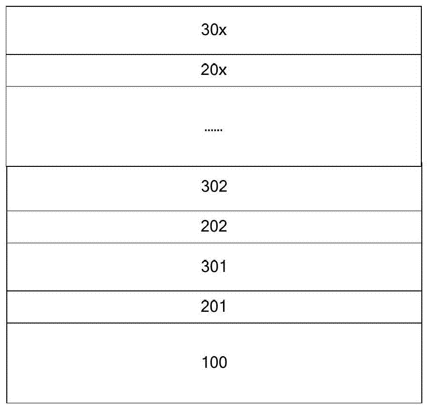
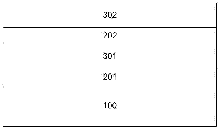
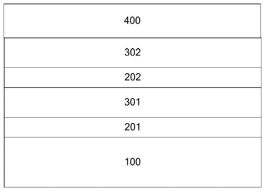
[0031]Embodiments of the present invention are described in detail below, examples of which are shown in the drawings, wherein the same or similar reference numerals designate the same or similar elements or elements having the same or similar functions throughout. The embodiments described below by referring to the figures are exemplary only for explaining the present invention and should not be construed as limiting the present invention.

[0032] In describing the present invention, it should be understood that the terms "center", "longitudinal", "transverse", "upper", "lower", "front", "rear", "left", "right", " The orientations or positional relationships indicated by "vertical", "horizontal", "top", "bottom", "inner", "outer", etc. are based on the orientation or positional relationships shown in the drawings, and are only for the convenience of describing the present invention and simplifying Describes, but does not indicate or imply that the device or element referred ...


PUM


Abstract

The invention provides a semiconductor structure with a rare earth oxide. The semiconductor structure comprises a semiconductor substrate, and multiple isolation oxide layers and multiple single crystal semiconductor layers which are formed on the semiconductor substrate and are alternately stacked, wherein the materials of the isolation oxide layer contacted with the semiconductor substrate are rare earth oxide or silicon dioxide, and the materials of other isolation oxide layers are single crystal rare earth oxide. According to the semiconductor structure provided by the embodiment of the invention, through lattice matching between the isolation oxide layers and the single crystal semiconductor layers, the crystal defect of the semiconductor structure can be obviously reduced, so that a three-dimensional semiconductor device with high performance and high density can be further formed on the semiconductor structure, the integrated density of the device is greatly improved, and simultaneously, the three-dimensional integration of different devices can also be realized.

Description

technical field [0001] The invention relates to the field of semiconductors, in particular to a semiconductor structure with rare earth oxides. Background technique [0002] In the field of semiconductors, in order to obtain highly integrated chips, the use of three-dimensional structures is one of the development directions. For example, a memory chip with a multi-layer stack structure is an important technical trend of high-density storage technology at present. In order to prepare a multilayer stacked device structure, one of the methods is to first prepare a semiconductor structure in which multiple layers of insulating dielectric layers and multiple layers of single crystal semiconductor layers are alternately stacked, and then prepare devices on the single crystal semiconductor layer. However, there has been no significant progress in the fabrication technology of a semiconductor structure having an alternately stacked structure of multiple layers of insulating dielec...

Claims


Application Information

Patent Timeline
Patent Type & Authority Applications(China)
IPC IPC(8): H01L29/06H01L29/24
CPCH01L29/02H01L21/28255H01L29/517H01L29/78H01L29/1054H01L29/161H01L21/02507H01L21/0251
Inventor 王敬梁仁荣郭磊许军
Owner TSINGHUA UNIV
Why Eureka
Try Eureka