A kind of thin film structure transparent electrode and preparation method thereof
A technology of transparent electrodes and thin-film structures, applied in circuits, electrical components, semiconductor devices, etc., can solve the problems affecting the quality of contact and the increase of contact interface defects, and achieve the effects of improving work efficiency, excellent performance, good quality, and high melting point
- Summary
- Abstract
- Description
- Claims
- Application Information
AI Technical Summary
Problems solved by technology
Method used
Image
Examples
Embodiment 1
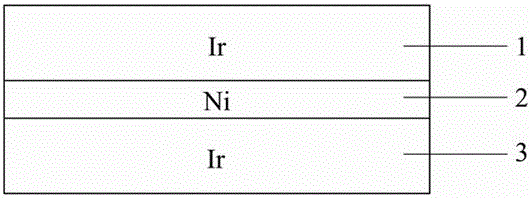
[0037] Such as figure 1 As shown, the present invention discloses a thin-film structure transparent electrode comprising metallic iridium forming a Schottky contact with an n-type semiconductor.
[0038] Further, metal iridium is added to metal iridium to form metal iridium-metal nickel-metal iridium; the thicknesses of each layer are respectively:
[0039] Metal iridium: 5-120 nm
[0040] Metal nickel: 1-40 nm
[0041] Metal iridium: 5-120 nm
[0042] The preparation process can adopt methods such as sputtering or electron beam evaporation, and the transparent electrode can be used to form an ohmic contact on the semiconductor material.
[0043] In order to achieve the above object, taking the electron beam evaporation method as an example, the present invention can be prepared by the following steps:
[0044] A. The mask layer is prepared by photolithography technology, so that the part of the semiconductor surface and the metal electrode is exposed, and the rest is cove...
Embodiment 2
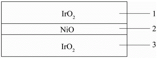
[0050] Such as figure 2 As shown, the present invention discloses an iridium oxide that forms an ohmic contact with a p-type semiconductor.
[0051] Further, nickel oxide is added to iridium oxide to form iridium oxide-nickel oxide-iridium oxide. The thickness of each layer is:
[0052] Iridium Oxide: 5-120 nm
[0054] Iridium Oxide: 5-120 nm
[0055] The preparation process may adopt methods such as sputtering or electron beam evaporation, and then oxidize in an oxygen or air atmosphere. The transparent electrode can be used to form a Schottky contact on the semiconductor material.
[0056] Taking the electron beam evaporation method as an example, the preparation method is similar to that of Example 1, steps A, B, and C are the same, and in step D, the alloy is carried out in oxygen or air.
PUM
| Property | Measurement | Unit |
|---|---|---|
| thickness | aaaaa | aaaaa |
| thickness | aaaaa | aaaaa |
| melting point | aaaaa | aaaaa |
Abstract
Description
Claims
Application Information

