Thin film structure transparent electrode and preparation method thereof

A technology of transparent electrodes and thin-film structures, which is applied in the direction of circuits, electrical components, semiconductor devices, etc., can solve the problems of affecting the quality of contact and increasing the number of defects in the contact interface, and achieve improved work efficiency, excellent performance, good quality, and long service life. Effect

Inactive Publication Date: 2013-02-06
SUN YAT SEN UNIV
View PDF4 Cites 2 Cited by
  • Summary
  • Abstract
  • Description
  • Claims
  • Application Information

AI Technical Summary

Problems solved by technology

But in fact, during the contact annealing process, the group III metal atoms (such as Ga, Al, In) and N atoms in the GaN-based material will diffuse outward and escape, resulting in the increase of metal-semiconductor contact interface defects, which greatly affects the contact quality. quality

Method used


Image

  • Thin film structure transparent electrode and preparation method thereof
  • Thin film structure transparent electrode and preparation method thereof

Examples


Embodiment 1

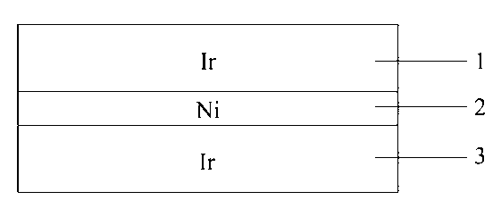
[0037] like figure 1 As shown, the present invention discloses a thin-film structure transparent electrode comprising metallic iridium forming a Schottky contact with an n-type semiconductor.

[0038] Further, metal iridium is added to metal iridium to form metal iridium-metal nickel-metal iridium; the thicknesses of each layer are respectively:

[0039] Metal iridium: 5-120 nm

[0040] Metal nickel: 1-40 nm

[0041] Metal iridium: 5-120 nm

[0042] The preparation process can adopt methods such as sputtering or electron beam evaporation, and the transparent electrode can be used to form an ohmic contact on the semiconductor material.

[0043] In order to achieve the above object, taking the electron beam evaporation method as an example, the present invention can be prepared by the following steps:

[0044] A. The mask layer is prepared by photolithography technology, so that the part of the semiconductor surface and the metal electrode is exposed, and the rest is cove...

Embodiment 2

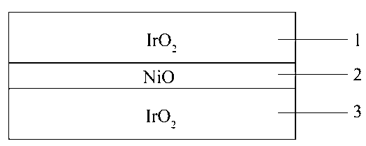
[0050] like figure 2 As shown, the present invention discloses an iridium oxide that forms an ohmic contact with a p-type semiconductor.

[0051] Further, nickel oxide is added to iridium oxide to form iridium oxide-nickel oxide-iridium oxide. The thickness of each layer is:

[0052] Iridium Oxide: 5-120 nm

[0053] Nickel Oxide: 1-40 nm

[0054] Iridium Oxide: 5-120 nm

[0055] The preparation process may adopt methods such as sputtering or electron beam evaporation, and then oxidize in an oxygen or air atmosphere. The transparent electrode can be used to form a Schottky contact on the semiconductor material.

[0056] Taking the electron beam evaporation method as an example, the preparation method is similar to that of Example 1, steps A, B, and C are the same, and in step D, the alloy is carried out in oxygen or air.


PUM

PropertyMeasurementUnit
thicknessaaaaaaaaaa
thicknessaaaaaaaaaa
melting pointaaaaaaaaaa

Abstract

The invention discloses a thin film structure transparent electrode and a preparation method thereof. The thin film structure transparent electrode comprises a metal iridium in Schottky contact with an n-type semiconductor or iridium oxide in ohmic contact with a p-type semiconductor; a metal nickel is added into the metal iridium to form a metal iridium-metal nickel-metal iridium product; and nickel oxide is added into the iridium oxide to form an iridium oxide-nickel oxide-iridium oxide product. The thin film structure transparent electrode has the advantages of large metal work function, high melting point, good heat stability, good light transmittance, strong corrosion resistance, excellent resistance to oxidation and the like.

Description

technical field [0001] The invention relates to a thin film structure transparent electrode and a preparation method thereof. Background technique [0002] Due to its excellent photoelectric properties, transparent conductive films have important applications in the fields of optical display devices, photodetection devices, solar cells, touch panels, and electrochromic devices. For light display devices, such as light-emitting diodes, the use of thin-film transparent electrodes can increase the light extraction efficiency and help improve the performance of light-emitting diodes; for photodetection devices, thin-film transparent electrodes can increase the amount of light received by the device and improve the sensitivity of the detector . [0003] Group III nitrides belong to the third generation of semiconductors and are typical wide bandgap compound semiconductor materials. GaN-based materials (including its binary compounds GaN, InN, and AlN, ternary compounds InGaN, A...

Claims


Application Information

Patent Timeline
Patent Type & Authority Applications(China)
IPC IPC(8): H01L33/42H01L33/00
Inventor 江灏伍伟聪李剑飞
Owner SUN YAT SEN UNIV
Why Eureka
Try Eureka