
System for treating laser coating

A coating and laser technology, applied in laser welding equipment, manufacturing tools, welding equipment, etc., can solve the problems of difficulty in forming complex and fine patterns, slow coating processing speed, etc., to achieve optimized heat absorption, improved flow conditions, and high processing quality effect

Active Publication Date: 2015-06-03
INST OF SEMICONDUCTORS - CHINESE ACAD OF SCI
View PDF5 Cites 0 Cited by
  • Summary
  • Abstract
  • Description
  • Claims
  • Application Information

AI Technical Summary

Problems solved by technology

[0003] Ordinary plating process occurs on the entire electrode substrate, the plating process is slow, and it is difficult to form complex and fine patterns

Method used


Image

  • System for treating laser coating
  • System for treating laser coating
  • System for treating laser coating

Examples


Embodiment 1

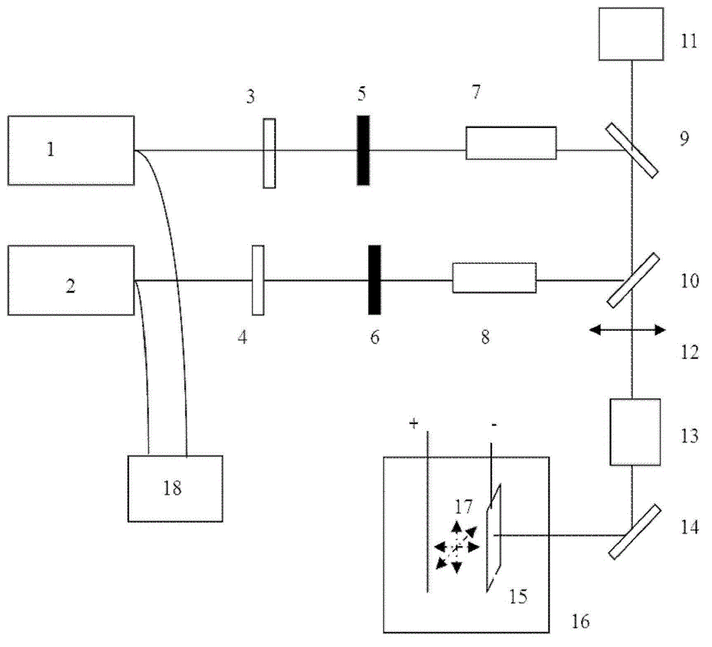
[0073] Example 1 is combined figure 1 The method for processing the laser coating provided by the present invention is described in detail.

[0074] The first pulse laser 1 is a Q-switched YAG frequency-doubled laser. The output laser beam has a wavelength of 532nm, an average power of 350mW, a pulse width of 100ns, a focused spot diameter of 500um, and an operating frequency of 200KHz; the second pulse laser 2 is Q-switched. The wavelength of the laser beam output by the YAG frequency doubled laser is 355nm, the average power is 200mW, the pulse width is 50ns, the spot diameter after focusing is 300um, and the working frequency is 200KHz.

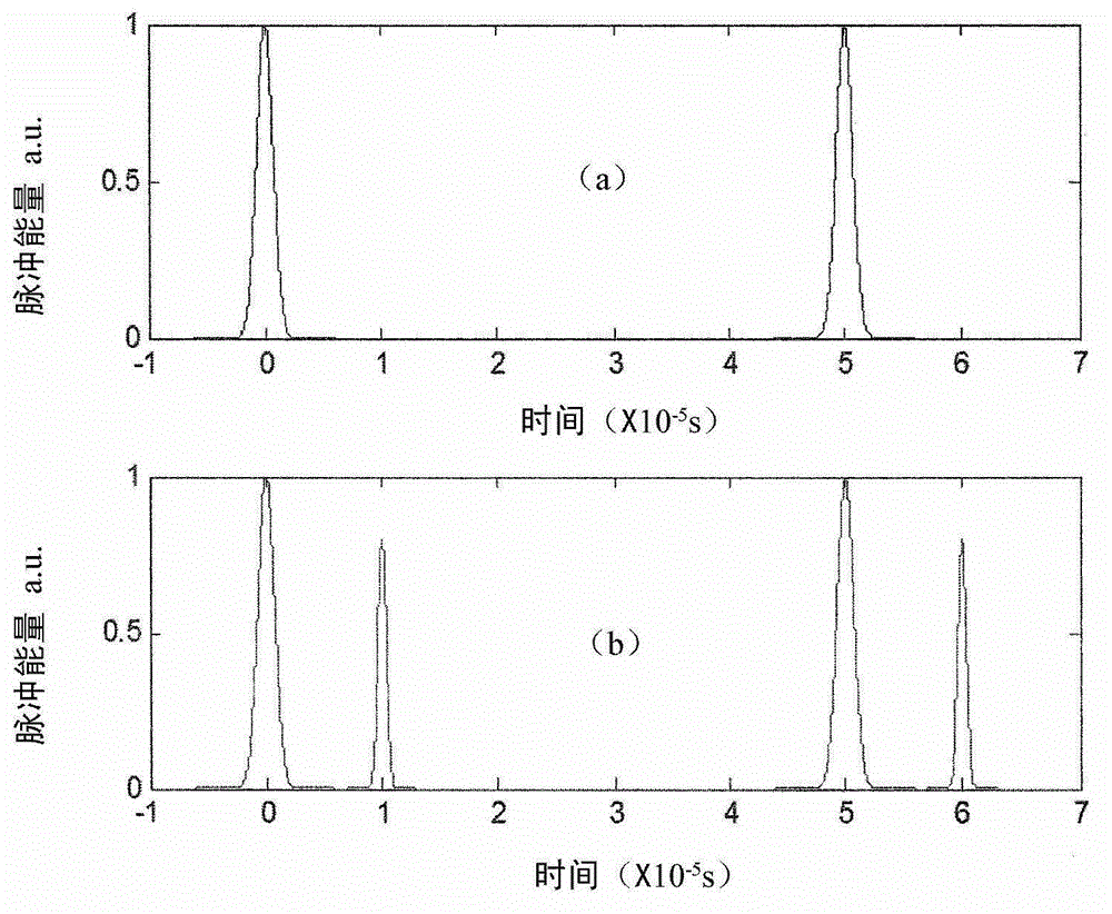
[0075] The first pulse laser 1 and the second pulse laser 2 are connected to a delay controller 18, and the delay controller 18 controls the interval between the first pulse emitted by the first pulse laser 1 and the second pulse emitted by the second pulse laser 2 by means of electrical modulation. There is a time delay which is 100ns. ...

Embodiment 2

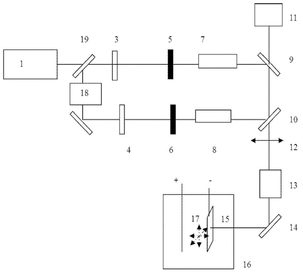
[0078] Example 2 is combined figure 2 The method for processing the laser coating provided by the present invention is described in detail.

[0079] The first pulse laser 1 is a Q-switched YAG frequency-doubled laser outputting a laser beam with a wavelength of 532nm, an average power of 350mW, a pulse width of 50ns, a spot diameter of 500um after focusing, and an operating frequency of 200kHz. Adopt the beam splitter 19 to split the second laser beam, utilize the spatial optical time retarder, adjust image 3 The relative positions of the two pairs of mirrors are such that the interval between the first laser pulse and the second laser pulse is 100 ns. Other operation steps are with embodiment 1

[0080] The invention provides a system for processing the laser coating, which realizes the fine processing of the laser coating. The laser fine processing method and system can be precisely controlled by laser coating processing. By using the laser beam with pulse and waveleng...


PUM

PropertyMeasurementUnit
wavelengthaaaaaaaaaa

Abstract

The invention discloses a system for treating a laser coating. The system comprises a first pulse laser (1), a second pulse laser (2), a first attenuator (3), a second attenuator (4), a first electronic shutter (5), a second electronic shutter (6), a first beam expanding lens (7), a second beam expanding lens (8), a reflector (9), a beam combiner (10), a CCD (Charge Coupled Device) real-time observation system (11), an optical galvanometer (12), a focus objective lens (13), a reflector (14), a pending sample substrate (15), an electrolytic cell (16), a three-dimensional mobile station (17) and a delay controller (18). According to the invention, a laser heat effect is fully absorbed by a material through utilizing pulse matched with the absorptive character of the material to be treated, and a laser beam of the wavelength, so that an ideal coating treatment result is obtained. The system, provided by the invention, is used for a treating process including laser electroplating, laser chemical plating, laser etching and micro laser cladding.

Description

technical field [0001] The invention relates to the technical field of laser coating processing, in particular to a system for processing laser coatings, which has a high degree of freedom in controlling the thickness of the coating and the width of the coating line, and can obtain fine coating quality. The invention is applicable to the treatment processes of laser electroplating, laser chemical plating, laser etching and laser micro-melting. Background technique [0002] Due to the incomparable advantages of laser, such as high energy density, high monochromaticity, good coherence and directionality, etc., its application in surface treatment technology is becoming more and more attractive. Laser-induced coating treatment on metals, semiconductors and polymers has attracted great attention in recent years. This process has broad application prospects in the fabrication and repair of microelectronic circuits. [0003] Ordinary plating treatment occurs on the entire electro...

Claims


Application Information

Patent Timeline
Patent Type & Authority Patents(China)
IPC IPC(8): C25D5/00C25D5/18C23C18/31C23C24/10B23K26/352
Inventor 林学春杨盈莹赵树森于海娟
Owner INST OF SEMICONDUCTORS - CHINESE ACAD OF SCI
Learn More