

Method for testing proton/single event effect resisting capacity of device
A single event effect, proton technology, applied in the direction of electronic circuit testing, non-contact circuit testing, etc., can solve the problem that the ability of anti-proton single event effect is not accurate and sensitive, and achieve the effect of convenient processing
- Summary
- Abstract
- Description
- Claims
- Application Information
AI Technical Summary
Problems solved by technology
Method used
Image

Examples
Embodiment Construction
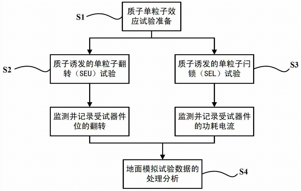
[0042] The method for testing the anti-proton single event effect of the device proposed by the present invention is described as follows in conjunction with the accompanying drawings and examples.
[0043] Such as figure 1 Shown, proton single event effect ground simulation test method of the present invention comprises steps:
[0044] S1.1. Preparations before the proton single event effect test, prepare the device to be tested and put forward the proton single event effect test requirements;
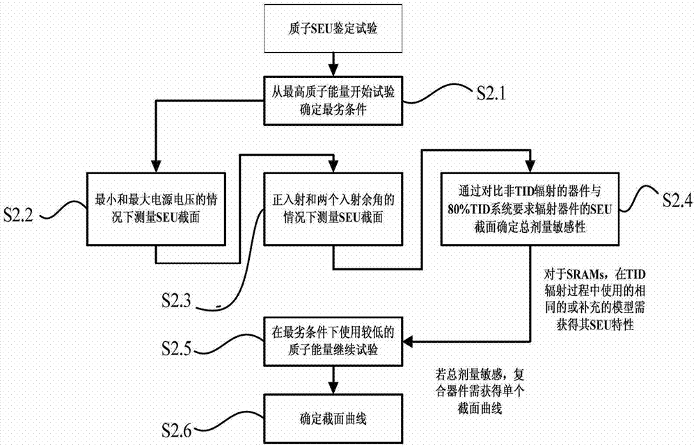
[0045] S2.1. The second step is to conduct proton-induced single event upset (SEU) test, monitor and record the reversal of the tested device position;
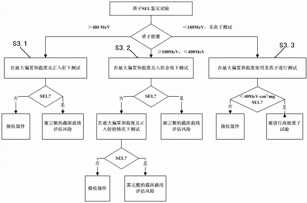
[0046] S2.2. Perform a proton-induced single event latch-up test (SEL), monitor and record the power consumption current of the device under test;
[0047] S3.1. According to the inversion data and the current and power consumption of the device, the processing and analysis of the experimental data is carried out to obtain the anti...
PUM
 Abstract
Description
Claims
Application Information