Manufacture method of optical printed wiring board

A manufacturing method and optical printing technology, which is applied to the coupling of printed circuit components and optical waveguides, can solve problems such as limiting system performance, and achieve the effect of low transmission loss

Inactive Publication Date: 2013-02-13
ELEC & ELTEK GUANGZHOU ELECTRONICS +1
View PDF6 Cites 11 Cited by
  • Summary
  • Abstract
  • Description
  • Claims
  • Application Information

AI Technical Summary

Problems solved by technology

[0002] As future computer systems increasingly require higher transmission requirements, traditional printed circuit board (PCB) metal-based electronic circuits are limited by physical limitations, such as signal interference, impedance matching, transmission loss, etc. performance of the entire system

Method used


Image

  • Manufacture method of optical printed wiring board
  • Manufacture method of optical printed wiring board
  • Manufacture method of optical printed wiring board

Examples


Embodiment Construction

[0026] Below in conjunction with accompanying drawing, preferred embodiment of the present invention is described in further detail:

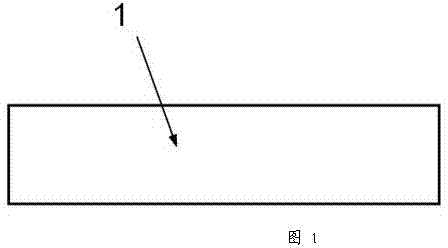
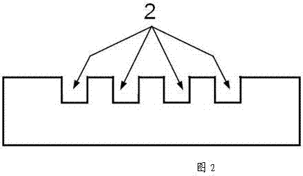
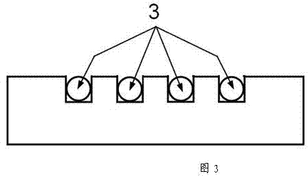
[0027] Such as Figures 1 to 4 As mentioned above, first prepare a clean FR4 sheet (glass fiber epoxy resin copper clad laminate) 1, such as figure 1 as shown, and then make groove 2, such as figure 2 As shown, the cross-sectional size of the groove is the diameter of the standard optical fiber 3, and then place the optical fiber 3 in the groove 2, such as image 3 shown. Finally, after the pressing process, the optical fiber 3 will be embedded in the printed circuit board to form an optical layer, and the general copper lines 4 can continue to be distributed on the surface of the circuit board, such as Figure 4 shown.

[0028] refer to Figure 5 , After forming the optical layer, the most critical issue is how to couple the light in and out, and how to turn the light by total reflection. Using the above-mentioned bevel cutting method, ...


PUM


Abstract

The invention provides a manufacture method of an optical printed wiring board. The manufacture method of the optical printed wiring board includes the following steps: a step of opening a groove, a step of pressing a plate, a step of cutting out an angle, a step of polishing a laser surface and a step of drilling a hole on the back. The manufacture method of the optical printed wiring board has the advantages that a bottleneck of electric mutual connection broadcasting brand width on a conventional printed wiring board is broken through and signal broadcasting brand width can be higher than 10 gigabytes / second. Besides, conventional optical components such as a vertical cavity face emitting laser device. An optical sensor and the like can be also inserted on a wiring board face. The wiring board face is compatible with an existing surface mount technology and the development potential for mass production.

Description

technical field [0001] The invention relates to an optical printed circuit board. Background technique [0002] As future computer systems increasingly require higher transmission requirements, traditional printed circuit board (PCB) metal-based electronic circuits are limited by physical limitations, such as signal interference, impedance matching, transmission loss, etc. performance of the entire system. Contents of the invention [0003] In order to solve the above technical problems, the present invention provides a method for manufacturing an optical printed circuit board, comprising the following steps: slotting step, plate pressing step, angle cutting step, laser surface grinding step, and backside drilling step. [0004] Optical printed circuit board is a solution for high-speed transmission. It can use light waves as the medium of signal transmission, and can provide data rates above 10Gb / s, and has the advantages of low power consumption and immunity to electrom...

Claims


Application Information

Patent Timeline
Patent Type & Authority Applications(China)
IPC IPC(8): G02B6/43H05K1/02
Inventor 杜子良罗家邦
Owner ELEC & ELTEK GUANGZHOU ELECTRONICS
Why Eureka
Try Eureka