A method of manufacturing an LED package

A LED packaging body and LED packaging technology, which is applied to semiconductor devices, electrical components, circuits, etc., can solve the problems of large amount of phosphor powder and uneven coating of phosphor powder, and achieve the effect of flexible and convenient operation

Active Publication Date: 2016-05-11
北京半导体照明科技促进中心
View PDF5 Cites 0 Cited by
  • Summary
  • Abstract
  • Description
  • Claims
  • Application Information

AI Technical Summary

Problems solved by technology

[0004] The purpose of the present invention is to provide a method for manufacturing an LED package to solve the problem of fluorescence existing in the coating of phosphor powder by means of dispensing, spraying or silk screen printing after completing the mechanical fixing and electrical connection of the LED chip in the prior art. Technical problems of uneven powder coating or large amount of phosphor powder

Method used


Image

  • A method of manufacturing an LED package
  • A method of manufacturing an LED package
  • A method of manufacturing an LED package

Examples


Embodiment 1

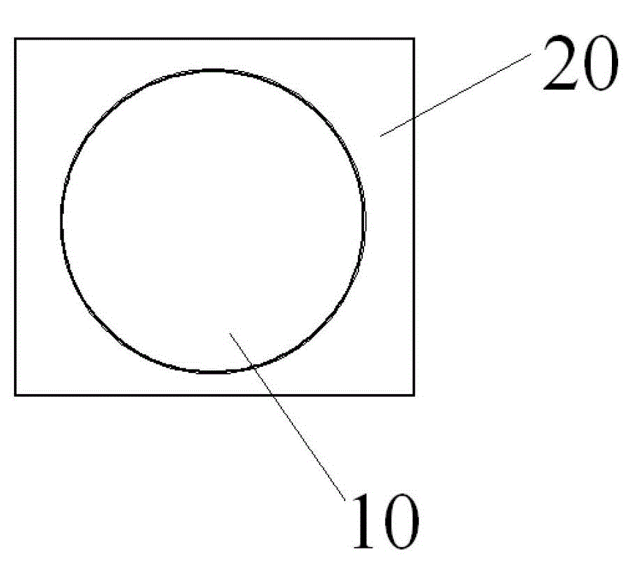
[0032] 1) if figure 1 As shown, the LED wafer 10 is fixed on the adhesive film 20 (the electrode pins are stuck on the adhesive film, figure 1 not shown in );

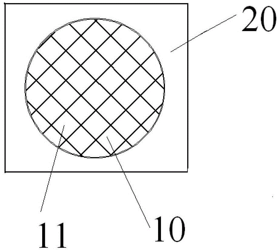
[0033] 2) Carry out cutting to obtain LED chips 11 of suitable size, such as figure 2 shown;

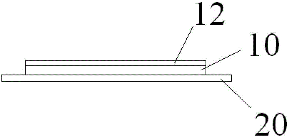
[0034] 3) Spray, brush, roll or screen-print phosphor glue, or press thermoplastic curing glue to apply phosphor-containing glue to the above-mentioned entire board of LED chips 11 on the adhesive film, and bake Curing to obtain a whole board of LED chips 11 uniformly coated with phosphor powder, such as image 3 shown;

[0035] 4) Carry out crystal expansion treatment on the entire board LED chip 11 evenly coated with phosphor powder on the adhesive film, such as Figure 4 As shown, the LED chip 11 provided with the phosphor layer 12 is obtained;

[0036] 5) Encapsulate the LED chip 11 provided with the phosphor layer 12; wherein, the encapsulation may include the following steps: cleaning the encapsulation substrate,...

Embodiment 2

[0038] 1) if figure 1As shown, the LED wafer 10 is fixed on the adhesive film 20 (the electrode pins are stuck on the adhesive film, figure 1 not shown in ),

[0039] 2) Carry out cutting to obtain LED chips 11 of suitable size, such as figure 2 shown;

[0040] 3) Carry out crystal expansion treatment on the entire board of LED chips 11 on the adhesive film, such as Figure 4 shown;

[0041] 4) Apply phosphor-containing glue to the entire LED chip 11 on the adhesive film by spraying, brushing, rolling or screen-printing phosphor glue, or pressing thermoplastic curing glue, and bake Curing to obtain the whole board LED chip 11 uniformly coated with phosphor layer 12, such as image 3 Shown; The LED chip 11 that obtains after cutting is as Figure 5 As shown, wherein the fluorescent layer 12 covers the surface of the LED chip 11;

[0042] 5) Encapsulate the LED chip 11 provided with the phosphor layer 12; wherein, the encapsulation may include the following steps: cleani...


PUM


Abstract

The invention discloses a manufacturing method of an LED (Light-Emitting Diode) packaging body. The preparation method comprises the following steps of: preparing an LED chip provided with a fluorescent powder layer; and then, packaging the LED chip provided with the fluorescent powder layer. With the adoption of the technical scheme, the fluorescent powder layer of the LED chip is arranged before package so that the operation is more convenient and the operation manner is more flexible. A technicist of the field can set the fluorescent powder layer on a whole board LED after an LED wafer is sliced and before the package; the set area is larger so that uniform coating can be carried out; and a phenomenon that the distribution is not uniform, caused by the influence of surface tension, is not caused, so that the technical problem in the prior art that fluorescent powder is not uniformly coated or the use amount of the fluorescent powder is large is effectively avoided.

Description

technical field [0001] The invention relates to the technical field of semiconductor preparation, in particular to a method for manufacturing an LED package. Background technique [0002] During the preparation of LED chips, the thickness of the phosphor layer seriously affects the luminous efficiency of the phosphor and the final light effect of the product, and the uniformity of its distribution will also have a greater impact on the consistency and yield of the product. The coating process has a great influence on the LED manufacturing process. [0003] At present, the traditional coating process of phosphor powder is to complete the coating of phosphor powder by dispensing, spraying or silk screen printing after the LED chip is mechanically fixed and electrically connected. Among them, the dispensing method has the following deficiencies: ① After the glue containing phosphor is baked, it will form an arc-shaped structure with a thick middle and a thin periphery on the s...

Claims


Application Information

Patent Timeline
Patent Type & Authority Patents(China)
IPC IPC(8): H01L33/50
Inventor 崔成强黄洁莹梁润园袁长安张国旗
Owner 北京半导体照明科技促进中心
Why Eureka
Try Eureka