Highly abrasion-resistant imprint material

A technology of base material and polymeric group, applied in the field of imprinting materials, to achieve the effect of expanding the process margin

Active Publication Date: 2013-02-20
NISSAN CHEM IND LTD
View PDF6 Cites 6 Cited by
  • Summary
  • Abstract
  • Description
  • Claims
  • Application Information

AI Technical Summary

Problems solved by technology

), but it can be said that there is no report of a material that maintains high scratch resistance after performing a scratch test after making a structure such as a concave-convex pattern.

Method used


Image

  • Highly abrasion-resistant imprint material
  • Highly abrasion-resistant imprint material

Examples


Embodiment

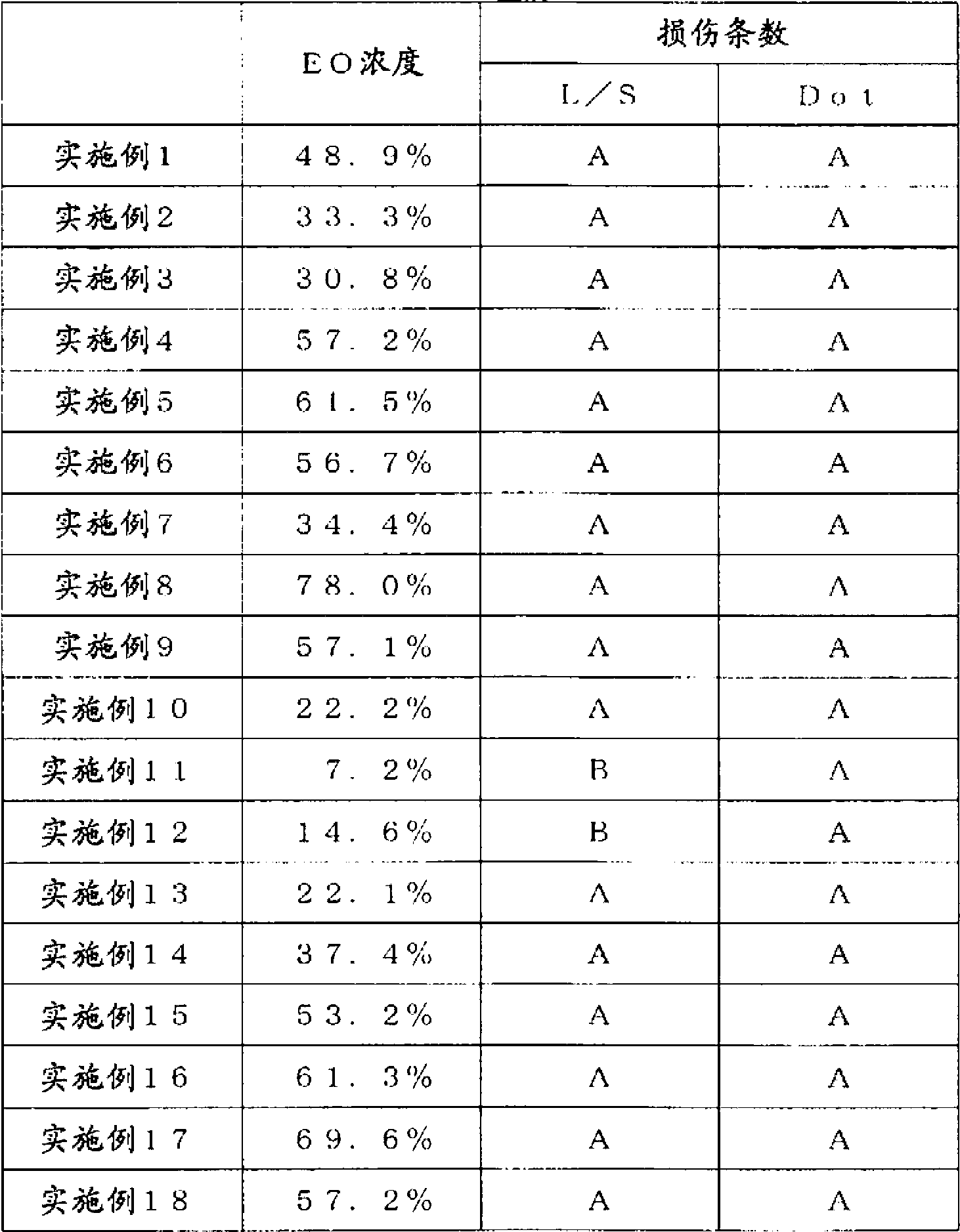
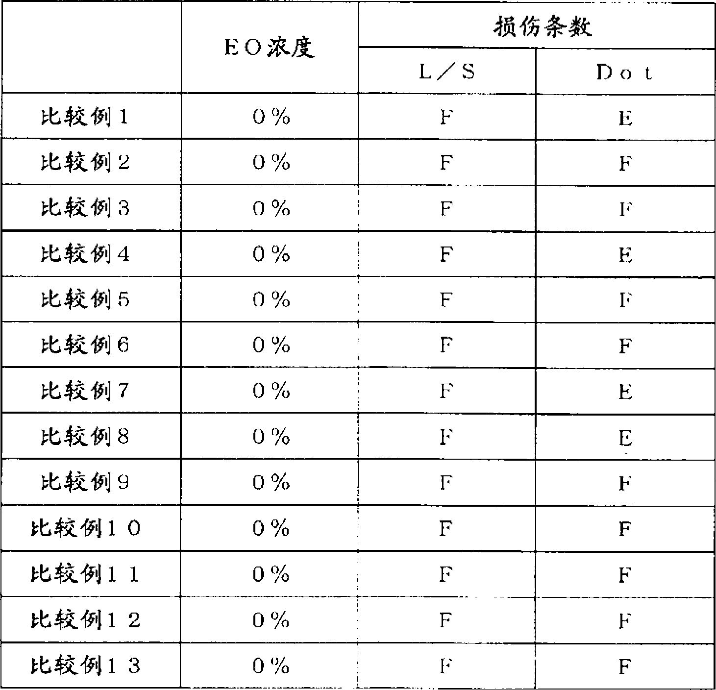
[0073] Hereinafter, although an Example and a comparative example are given and this invention is demonstrated in detail, this invention is not limited to these Examples.

[0074] [Preparation of coating solution for film formation]

[0075]

[0076] DAROCUR (registered trademark) 1173 (BASF Japan Co., Ltd. Co., Ltd.) (hereinafter, abbreviated as “DAROCUR1173” in this specification.) 1 g (20 phr relative to the total mass of DPEA-12), and an imprint material PNI-A1 was prepared. In the present example, DPEA-12 corresponds to the component (A), and the number of oxyalkylene units per molecule is 12 EO (ethylene oxide units). DAROCUR1173 corresponds to (B) component.

Embodiment 2

[0078] DPEA-12 of Example 1 was changed to NK Ester ATM-4E (manufactured by Shin Nakamura Chemical Industry Co., Ltd., molecular weight: 529) (hereinafter, abbreviated as "ATM-4E" in this specification.), in addition, the same as In the same manner as in Example 1, an imprint material PNI-A2 was prepared. In the present example, ATM-4E corresponds to the component (A), and the number of oxyalkylene units per molecule is four EO.

Embodiment 3

[0080] DPEA-12 of Example 1 was changed to NK Ester A-TMPT-3EO (manufactured by Shin Nakamura Chemical Industry Co., Ltd., molecular weight: 428) (hereinafter, abbreviated as "A-TMPT-3EO" in this specification.), except Otherwise, it carried out similarly to Example 1, and prepared the imprint material PNI-A3. In the present example, A-TMPT-3EO corresponds to the component (A), and the number of oxyalkylene units per molecule is three EO.


PUM


Abstract

Provided is a highly abrasion-resistant imprint material. The imprint material comprises a compound that has C2-3 alkylene oxide units and at least two polymerizable groups as component (A) and a photopolymerization initiator as component (B). The polymerizable groups are at least one selected from the group consisting of acryloyloxy, acryloyl, methacryloyloxy, and methacryloyl groups. The imprint material can further comprise, in addition to component (A), a compound that has at least two polymerizable groups but does not have C2-3 alkylene oxide units as component (A').

Description

technical field [0001] The present invention relates to embossed materials, and films produced from the materials and transferred with patterns. More specifically, it relates to an imprint material having high scratch resistance even after a pattern has been transferred, and a film produced from the material and transferred with a pattern. Background technique [0002] In 1995, a new technology called nanoimprint lithography was proposed by Professor Chiyo, now at Princeton University (Patent Document 1). Nanoimprint lithography is a process of bringing a mold having an arbitrary pattern into contact with a substrate on which a resin film is formed, pressing the resin film, and using heat or light as an external stimulus to form a target pattern on the cured resin film. This nanoimprint lithography has the advantage of being able to perform nanoscale processing easily and inexpensively compared with conventional photolithography in the manufacture of semiconductor devices. ...

Claims


Application Information

Patent Timeline
Patent Type & Authority Applications(China)
IPC IPC(8): H01L21/027C08F2/50C08F20/28C08F299/02
CPCC08F222/1006G03F7/0002G03F7/027H01L21/027B82Y10/00B82Y40/00C08F222/106C08F2/50C08F299/024H01L21/0274
Inventor 小林淳平加藤拓首藤圭介铃木正睦
Owner NISSAN CHEM IND LTD
Why Eureka
Try Eureka