Method for controlling uniformity of substrate oxide layer in manufacture procedure of shallow-channel insulation layer

A technology of insulating layer and shallow trench, which is applied in semiconductor/solid-state device manufacturing, electrical components, circuits, etc., can solve the problems of high cost, long cycle, uneven thickness, etc., to save production cost, shorten production time, Improve the effect of uneven thickness of substrate oxide layer

Active Publication Date: 2013-02-27
SHANGHAI HUALI MICROELECTRONICS CORP
View PDF4 Cites 2 Cited by
  • Summary
  • Abstract
  • Description
  • Claims
  • Application Information

AI Technical Summary

Problems solved by technology

This approach solves the problem of uneven thickness of the oxide film before ion implantation, but because the oxide layer needs to be regrown, it must go through a diffusion process, which has a long cycle and high cost.

Method used


Image

  • Method for controlling uniformity of substrate oxide layer in manufacture procedure of shallow-channel insulation layer
  • Method for controlling uniformity of substrate oxide layer in manufacture procedure of shallow-channel insulation layer
  • Method for controlling uniformity of substrate oxide layer in manufacture procedure of shallow-channel insulation layer

Examples


Embodiment Construction

[0020] The present invention will be further described below in conjunction with the accompanying drawings and specific embodiments, but not as a limitation of the present invention.

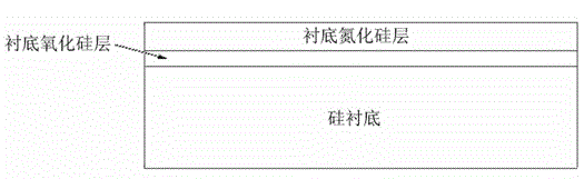
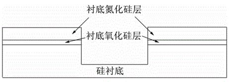
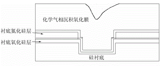
[0021] A method for controlling the uniformity of the substrate oxide layer in the shallow trench insulating layer process. This method is used in the shallow trench insulating layer (STI) process. The basic structure of STI is divided into three layers, from top to bottom: Substrate silicon nitride layer, substrate silicon oxide layer and silicon substrate; such as Figure 4 As shown, in one embodiment of the present invention, the specific steps of the method for controlling the uniformity of the substrate oxide layer in the shallow trench insulating layer process include:

[0022] Step a, growing a thin film with a certain thickness when growing the silicon oxide layer of the substrate; in this embodiment, the thickness of this thin film is tentatively set at 15 angstroms (1 angstrom=0.1 na...


PUM


Abstract

The invention discloses a method for controlling uniformity of a substrate oxide layer in a manufacture procedure of a shallow-channel insulation layer, which belongs to the technical field of technology of CMOS (complementary metal oxide semiconductor) semiconductor devices. The steps of the method are as follows: growing one more layer of thin film layer while growing a substrate silicon oxide layer, removing a substrate silicon nitride layer, measuring the thickness of the substrate silicon oxide layer after removing the substrate silicon nitride layer, taking the thickness as a front value, simultaneously setting a target value which is the thickness value of the substrate silicon oxide layer under an ideal condition, setting a modification value for the substrate silicon oxide layer in each batch, wherein the value range of the modification value is the difference range of the front value and the target value, and modifying and etching the substrate silicon oxide layer according to the modification value. The method adopting the technical scheme has the benefits that the problem of non-uniform thickness of the substrate oxide layers is improved, the manufacture cost of the semiconductor technology is saved, and the production-manufacturing time of a product is shortened.

Description

technical field [0001] The invention relates to the technical field of CMOS (Complementary Metal Oxide Semiconductor, Complementary Metal Oxide Semiconductor) semiconductor device technology, in particular to a method for controlling the uniformity of a substrate oxide layer in a shallow trench insulating layer manufacturing process. Background technique [0002] In the process of CMOS semiconductor devices, as the size of the device continues to shrink, the requirements for the process are getting higher and higher. The stability of wet etching is also becoming more and more important. [0003] In the current CMOS process, a shallow trench insulation (shallow trench isolation, STI) process is still widely used. like Figure 1.1-1.5 Shown is a block diagram of a typical STI process. first, Figure 1.1 shows the growth of substrate silicon oxide and substrate silicon nitride, followed by photolithography and dry etching to form as Figure 1.2 The STI pattern shown is form...

Claims


Application Information

Patent Timeline
Patent Type & Authority Applications(China)
IPC IPC(8): H01L21/8238H01L21/762
Inventor 王春伟李阳柏张传民张旭昇
Owner SHANGHAI HUALI MICROELECTRONICS CORP
Why Eureka
Try Eureka