Pixel circuit, driving method and display device of pixel circuit

A pixel circuit and voltage technology, applied in static indicators, instruments, etc., can solve the problems of OLED display device current difference, inconsistent threshold voltage offset, display brightness difference, etc., to achieve improved display effect, less quantity, and reduced area Effect

Active Publication Date: 2013-03-06
BOE TECH GRP CO LTD
View PDF5 Cites 13 Cited by
  • Summary
  • Abstract
  • Description
  • Claims
  • Application Information

AI Technical Summary

Problems solved by technology

However, due to the limitations of the crystallization process and manufacturing level, the TFT switch circuits fabricated on large-area glass substrates often have non-uniformity in electrical parameters such as threshold voltage and mobility, which makes the threshold voltage shift of each TFT inconsistent. , which will lead to current differences and brightness differences of OLED

Method used


Image

  • Pixel circuit, driving method and display device of pixel circuit
  • Pixel circuit, driving method and display device of pixel circuit
  • Pixel circuit, driving method and display device of pixel circuit

Examples


Example Embodiment

[0028] The technical solutions in the embodiments of the present invention will be clearly and completely described below in conjunction with the accompanying drawings in the embodiments of the present invention. Obviously, the described embodiments are only a part of the embodiments of the present invention, rather than all the embodiments. Based on the embodiments of the present invention, all other embodiments obtained by those of ordinary skill in the art without creative work shall fall within the protection scope of the present invention.

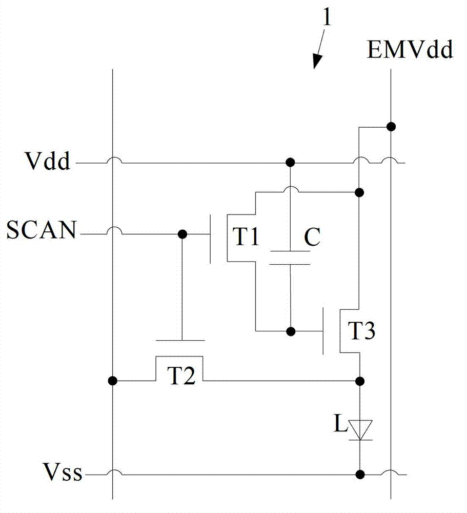
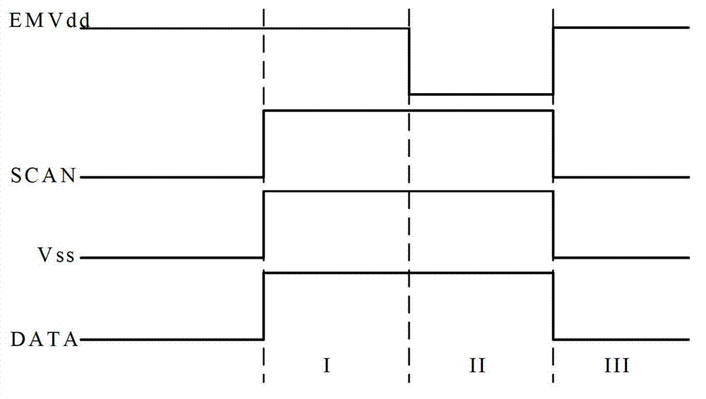
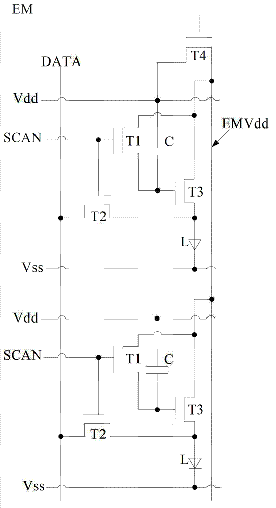
[0029] The pixel circuit 1 provided by the embodiment of the present invention, such as figure 1 Shown, including:

[0030] The first transistor T1, the second transistor T2, the storage capacitor C, and the third transistor T3 for driving the light emitting device L.

[0031] The gate of the first transistor T1 is connected to the scan line SCAN, the first electrode thereof is connected to the gate of the third transistor T3, and the second...


PUM


Abstract

The embodiment of the invention provides a pixel circuit, a driving method and a display device of the pixel circuit, relates to the field of display technology, can effectively compensate the threshold voltage shift of a thin film transistor (TFT) so as to improve the luminance homogeneity of the display device and improve the display effect. The pixel circuit comprises a first transistor, a second transistor, a memory capacitor and a third transistor for driving a luminescent device, wherein the grid electrode of the first transistor is connected with a scanning line; the first electrode of the first transistor is connected with the grid electrode of the third transistor; the second electrode of the first transistor is connected with a control power line; the grid electrode of the second transistor is connected with the scanning line; the first electrode is connected with a data line; the second electrode is connected with one end of the luminescent device; the first electrode of the third transistor is connected with the control power line; the second electrode is connected with one end of the luminescent device; one end of the memory capacitor is connected with a first power voltage; the other end of the memory capacitor is connected with the grid electrode of the third transistor; and the other end of the luminescent device is connected with a second power voltage. The embodiment is applied to manufacturing display panels.

Description

technical field [0001] The present invention relates to the field of display technology, in particular to a pixel circuit, a driving method thereof, and a display device. Background technique [0002] Organic Light Emitting Diode (OLED), as a current-mode light-emitting device, is increasingly being used because of its characteristics such as self-luminescence, fast response, wide viewing angle and the ability to be fabricated on flexible substrates. In the field of high-performance display. According to the driving method, OLED can be divided into two types: PMOLED (Passive Matrix Driving OLED, passive matrix driving organic light emitting diode) and AMOLED (Active Matrix Driving OLED, active matrix driving organic light emitting diode). As the size of the traditional PMOLED increases, the driving time of a single pixel usually needs to be reduced, so the transient current needs to be increased, resulting in a significant increase in power consumption. In the AMOLED techn...

Claims


Application Information

Patent Timeline
IPC IPC(8): G09G3/32G09G3/325
Inventor 宋丹娜吴仲远
Owner BOE TECH GRP CO LTD
Why Eureka
Try Eureka