Semiconductor device

A semiconductor and chip technology, applied in the direction of semiconductor devices, semiconductor/solid-state device parts, electric solid-state devices, etc., can solve the problem of low heat-resistant reliability and achieve the effect of improving heat-resistant reliability

Active Publication Date: 2013-03-06
SHINKO ELECTRIC IND CO LTD
View PDF4 Cites 15 Cited by
  • Summary
  • Abstract
  • Description
  • Claims
  • Application Information

AI Technical Summary

Problems solved by technology

Therefore, the conventional semiconductor device 3 has a problem of low heat resistance reliability.

Method used


Image

  • Semiconductor device
  • Semiconductor device
  • Semiconductor device

Examples


no. 1 Embodiment approach

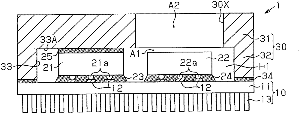
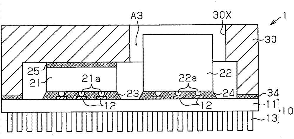
[0026] Below, refer to Figure 1 ~ Figure 3 , and the first embodiment will be described. Such as figure 1 As shown, the semiconductor device 1 has: a PGA (Pin Grid Array) type wiring board 10; a first semiconductor chip (first chip) 21 and a second semiconductor chip (second chip) 22, and these chips are mounted on the wiring substrate 10; On the wire substrate 10 ; the heat sink 30 is arranged on the first chip 21 . In the illustrated example, the first chip 21 and the second chip 22 are arranged in the horizontal direction (also referred to as a planar structure). Here, the first chip 21 is a logic chip, which has a high thermal resistance and generates a large amount of heat, and the second chip 22 is a memory chip, which has a lower thermal resistance than the first chip 21 and is not heat-resistant. The second chip 22 is a semiconductor chip whose heat generation is smaller than that of the first chip 21 . As the logic chip, for example, a CPU (Central Processing Un...

no. 2 Embodiment approach

[0052] Hereinafter, a second embodiment will be described with reference to FIG. 6 . right with the previous Figure 1 to Figure 5 Components that are the same as those shown are denoted by the same symbols, and detailed descriptions of the above-mentioned respective elements are omitted.

[0053] As shown in FIG. 6(a), the semiconductor device 2 has: a PGA (Pin Grid Array) type wiring substrate 10; The wiring board 10 ; the heat sink 30 is arranged on the first chip 21 ; the heat sink 40 is arranged on the second chip 22 ; and the heat insulating resin 41 is provided between the heat sink 30 and 40 .

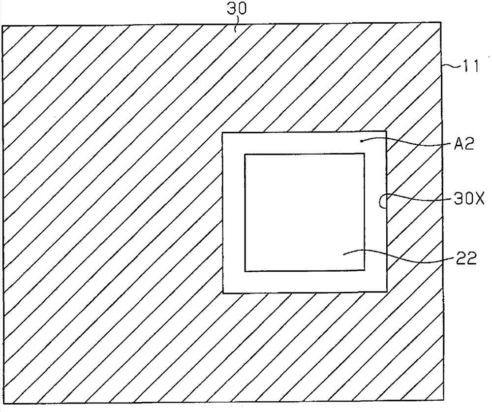
[0054] The upper surface of the first chip 21 is thermally coupled to the bottom surface 33A of the concave portion 33 of the heat sink 30 (first heat sink) through the thermal interface material 25 . On the heat sink 30 , at a position facing the second chip 22 , an opening 30X having a planar shape larger than that of the second chip 22 is formed.

[0055] The upper surfac...


PUM


Abstract

The present invention provides a semiconductor device (1) which can improve the hear resistance reliability. The semiconductor device includes a wiring substrate (10, 10A), a first semiconductor chip (21) mounted on the wiring substrate, and a second semiconductor chip (22) mounted on the wiring substrate. The second semiconductor chip generates less heat than the first semiconductor chip. A heat dissipation plate (30, 30A) is arranged on the wiring substrate and partially at a higher location than the first and second semiconductor chips. The heat dissipation plate is connected to the first semiconductor chip and includes an opening (30X) formed at a location corresponding to an upper surface of the second semiconductor chip. The upper surface of the second semiconductor chip is entirely exposed from the heat dissipation plate (30, 30A) through the opening (30).

Description

technical field [0001] The present invention relates to a semiconductor device. Background technique [0002] In recent years, there has been an increasing demand for miniaturization and higher functionality of semiconductor devices. A multi-chip package (Multi Chip Package: MCP) in which a plurality of semiconductor chips are mounted on one substrate is known as a semiconductor device capable of meeting such demands. [0003] In such a semiconductor device, a heat dissipation member (for example, a metal heat dissipation plate) for dissipating heat generated by the semiconductor chip to the atmosphere is arranged on the semiconductor chip. With this configuration, it is possible to ensure a passage for dissipating the heat generated by the semiconductor chip to the outside of the semiconductor device, thereby improving the heat dissipation of the semiconductor device. A thermal interface material (Thermal Interface Material: TIM) is interposed between the semiconductor ch...

Claims


Application Information

Patent Timeline
Patent Type & Authority Applications(China)
IPC IPC(8): H01L23/433
CPCH01L25/0655H01L23/36H01L23/42H01L23/3675H01L25/18H01L23/13H01L2224/73204H01L2224/16225H01L2224/32245H01L2224/32225H01L2924/16151H01L2224/73253H01L2924/16251H01L2924/16195H01L2924/15153H01L2924/00H01L23/31
Inventor 根来修司
Owner SHINKO ELECTRIC IND CO LTD
Why Eureka
Try Eureka